NEO-D0: Difference between revisions
Jump to navigation
Jump to search
(added note for typo, and corrected signal name) |
m (removed note because pinout has been corrected) |
||
| (One intermediate revision by the same user not shown) | |||
| Line 19: | Line 19: | ||
{{Pinout|NEO-D0|640}} | {{Pinout|NEO-D0|640}} | ||
=Internal schematic= | =Internal schematic= | ||
Latest revision as of 14:43, 21 May 2020

| |
| Package | QFP64R |
| Manufacturer | |
| First use | 1990 ? |
| Used on | MV4 and many more... |
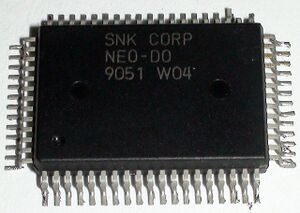
- Clock divider
- Z80 memory and port control
- YM2610 interface
- Memory card bank selection
- Joypad outputs
Maybe similar to NEO-SUD on the NeoGeo CD. Close to the audio hardware.
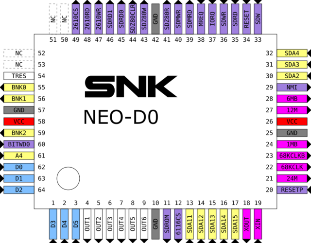
Pinout
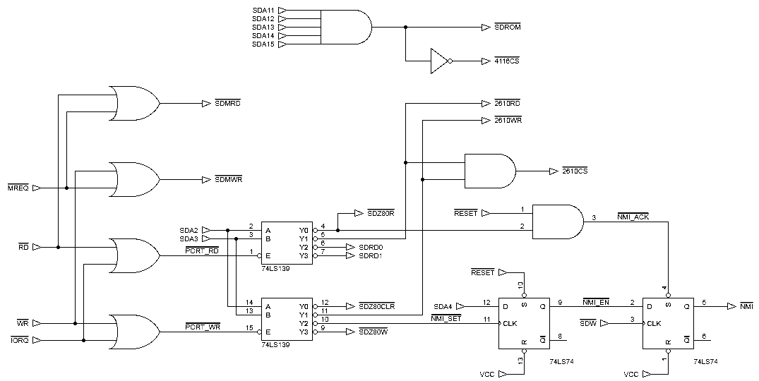
Internal schematic
Signals
- D*: 68k data bus for joypad outputs
- BNK*: Memory card upper address lines to NEO-E0
- A4: 68k address line for decoding
- 6116CS: Z80 RAM select
- 2610*: YM2610 control outputs
- OUT*: Joypad outputs
- SDMRD: Z80 ROM/RAM read
- SDMRW: Z80 RAM write
- SDRD*: Z80 port read to NEO-ZMC in cartridge
- SDZ80CLR: Clear command code in NEO-C1
- SDZ80RD: Read command code from NEO-C1
- SDZ80WR: Write reply code to NEO-C1

