MVS to AES adapter: Difference between revisions
mNo edit summary |
No edit summary |
||
| Line 1: | Line 1: | ||
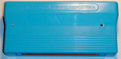
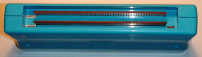
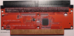
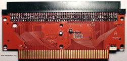
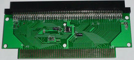
==NEO TEAM Super MVS Converter II PLUS V7== | |||
<div align="center"> | |||
<gallery widths=400px perrow=2> | |||
File:SMC2P.jpg | |||
File:SMC2P_ports.jpg | |||
File:SMC2P_progtop.jpg|Prog board top | |||
File:SMC2P_progbot.jpg|Prog board bottom | |||
File:SMC2P_chatop.jpg|CHA board top | |||
File:SMC2P_chabot.jpg|CHA board bottom | |||
</gallery> | |||
</div> | |||
[[File:SMC2P_fpga.jpg|thumb|left]] | |||
[[File:SMC2P_solder.jpg|thumb|Yuck !]] | |||
Uses an Actel ProASIC V3 FPGA on each board. They're AES-decryption capable for SPI flash and fusemap update, and generally highly temper-proof. | |||
Has two SPI ports for FPGA updates and one unrouted mini-USB port labelled "BIOS". | |||
Boards dated May 2011. Seems to suffer of very bad soldering job on connectors. | |||
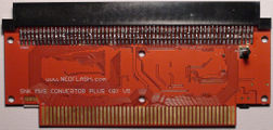
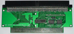
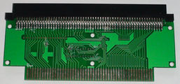
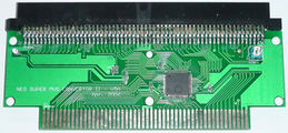
==NEO TEAM Super MVS Convertor II V5B== | ==NEO TEAM Super MVS Convertor II V5B== | ||
<div align="center"> | |||
<gallery widths=400px perrow=2> | |||
File:SMC2_progtop.jpg|Prog board top | |||
File:SMC2_progbot.jpg|Prog board bottom | |||
File:SMC2_chatop.jpg|CHA board top | |||
File:SMC2_chabot.jpg|CHA board bottom | |||
</gallery> | |||
</div> | |||
[[File:Neocellks300.jpg|thumb]] | |||
Uses a PAL18CV8 and two LS245 transceivers for the prog board. Two corresponding footprints for SIL pull-up resistors on the MVS side are left unpopulated. | Uses a PAL18CV8 and two LS245 transceivers for the prog board. Two corresponding footprints for SIL pull-up resistors on the MVS side are left unpopulated. | ||
Revision as of 20:30, 1 February 2012
NEO TEAM Super MVS Converter II PLUS V7
-
-
-
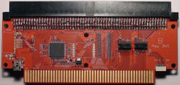
Prog board top
-
Prog board bottom
-
CHA board top
-
CHA board bottom


Uses an Actel ProASIC V3 FPGA on each board. They're AES-decryption capable for SPI flash and fusemap update, and generally highly temper-proof.
Has two SPI ports for FPGA updates and one unrouted mini-USB port labelled "BIOS".
Boards dated May 2011. Seems to suffer of very bad soldering job on connectors.
NEO TEAM Super MVS Convertor II V5B
-
Prog board top
-
Prog board bottom
-
CHA board top
-
CHA board bottom


Uses a PAL18CV8 and two LS245 transceivers for the prog board. Two corresponding footprints for SIL pull-up resistors on the MVS side are left unpopulated.
Uses a custom chip "NEO CELL KS300 8436020333002 06-03" to simulate NEO-ZMC2. An RC circuit (potentiometer) is used for CLK delay to make CMC games work correctly.
According to [these pictures], the chip would be a custom branded Altera MAX PLD. It's in fact en EPM240D (Boundary scan device ID reply with bus pirate: BB085040, reversed !) and the header on the back is for JTAG:
| TMS | TDO | GND |
| TDI | TCK | 3.3V |