NEO-B1: Difference between revisions
mNo edit summary |
mNo edit summary |
||
| Line 1: | Line 1: | ||
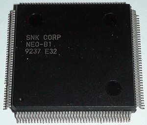
[[File:aes_b1.jpg|right|thumb|NEO-B1 chip found in an AES system.]] | [[File:aes_b1.jpg|right|thumb|NEO-B1 chip found in an AES system.]] | ||
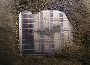
The NEO-B1 chip is found in second | [[File:b1die.jpg|right|thumb|(Damaged) B1 die showing memory cells.]] | ||
The NEO-B1 chip is found in second generation cartridge-based systems. | |||
==Graphics== | ==Graphics== | ||
Both FIX graphics from the [[S ROM]] and sprite graphics from the [[C ROM]] are fed to the NEO-B1 for display on screen. | Both FIX graphics from the [[S ROM]] and sprite graphics from the [[C ROM]] are fed to the NEO-B1 for display on screen via 2 pairs of alternating line buffers. Sprite graphics are sourced from the C ROM multiplexer ([[NEO-ZMC2]], [[PRO-CT0]] or [[NEO-CMC]]), while FIX graphics are sourced directly from the currently enabled FIX ROM. | ||
The [[palette RAM]] address lines are directly connected to | The [[palette RAM]] address lines are directly connected to NEO-B1 for pixel output. The data output of the palette RAM is latched by a pair of 8bit registers, which in turn output to the [[video DAC]]. The NEO-B1 arbitrates access to palette RAM and will pass the 68k address through to the palette RAM when reading/writing/testing the palette RAM. Priority is always given to the 68k which results in harmless display glitches when games access palette RAM while rendering the screen. | ||
==Watchdog== | ==Watchdog== | ||
The [[watchdog]] is integrated into the NEO-B1. | The [[watchdog]] is integrated into the NEO-B1. /HALT and /RESET are generated by this chip on power-on and whenever the 68k fails to write the watchdog register in time. It seems to decode the write to watchdog itself instead of using the [[NEO-C1]]. | ||
Watchdog can be disabled by bringing pin 94 DOGE to ground (J2 jumper on main board). | Watchdog can be disabled by bringing pin 94 DOGE to ground (J2 jumper on main board). | ||
Revision as of 09:00, 4 March 2014


The NEO-B1 chip is found in second generation cartridge-based systems.
Graphics
Both FIX graphics from the S ROM and sprite graphics from the C ROM are fed to the NEO-B1 for display on screen via 2 pairs of alternating line buffers. Sprite graphics are sourced from the C ROM multiplexer (NEO-ZMC2, PRO-CT0 or NEO-CMC), while FIX graphics are sourced directly from the currently enabled FIX ROM.
The palette RAM address lines are directly connected to NEO-B1 for pixel output. The data output of the palette RAM is latched by a pair of 8bit registers, which in turn output to the video DAC. The NEO-B1 arbitrates access to palette RAM and will pass the 68k address through to the palette RAM when reading/writing/testing the palette RAM. Priority is always given to the 68k which results in harmless display glitches when games access palette RAM while rendering the screen.
Watchdog
The watchdog is integrated into the NEO-B1. /HALT and /RESET are generated by this chip on power-on and whenever the 68k fails to write the watchdog register in time. It seems to decode the write to watchdog itself instead of using the NEO-C1.
Watchdog can be disabled by bringing pin 94 DOGE to ground (J2 jumper on main board).
Pinout
(Max size:File:neo-b1_pinout.png)
File:Neo-b1 pinout.png
OpenOffice Draw file: File:Neo-b1.odg
- A1~A21: 68k address bus
- A22I,A23I: 68k A22,A23 passed through NEO-E0
- FIX0~FIX7: FIX ROM data bus
- PCK1/PCK2: Latch signals, shared with LSPC2-A2 (inverted for NEO-273)
- PA0~PA11: Palette RAM address bus
- TDO0~TDO11: NC on the MV1F
- GAD0~GAD3: Pixel data from NEO-ZMC2
- GBD0~GBD3: Pixel data from NEO-ZMC2
- FLIP: Horizontal flip pixel line
- WE1~WE4: Write enable for pixel
- CK1~CK4: Stepping clocks
- SS1/SS2: ?
- LD1/LD2: Odd/Even scanline load ? Changes according to sprite list ?
- 1H1: 3MHz clock ?
- TMS0: Line buffer selection (0/1)
- DOGE: Watchdog enable (internal pullup)