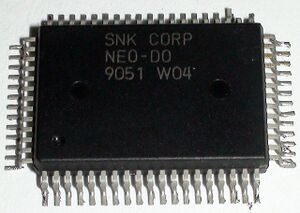
NEO-D0: Difference between revisions
Jump to navigation
Jump to search
mNo edit summary |
mNo edit summary |
||
| Line 1: | Line 1: | ||
[[File:aes_d0.jpg|right|thumb|NEO-D0 chip found on an AES board.]] | [[File:aes_d0.jpg|right|thumb|NEO-D0 chip found on an AES board.]] | ||
*Clock generation | |||
*[[YM2610]] control | |||
*Z80 port control (I/O to 68k and YM2610) | |||
*[[Memory card]] banking | |||
*Joypad outputs | |||
Probably similar to [[NEO-SUD]] on the NeoGeo CD. Close to the audio hardware. | Probably similar to [[NEO-SUD]] on the NeoGeo CD. Close to the audio hardware. | ||
Revision as of 06:48, 6 January 2013

- Clock generation
- YM2610 control
- Z80 port control (I/O to 68k and YM2610)
- Memory card banking
- Joypad outputs
Probably similar to NEO-SUD on the NeoGeo CD. Close to the audio hardware.
Pinouts
OpenOffice Draw file: File:Neo-d0.odg