NEO-E0: Difference between revisions
Jump to navigation
Jump to search
m (1 revision) |
mNo edit summary |
||
| (One intermediate revision by the same user not shown) | |||
| Line 2: | Line 2: | ||
Also found in MVS systems. Probably grouped glue logic, as early AES boards had plenty of 74HC chips instead. | Also found in MVS systems. Probably grouped glue logic, as early AES boards had plenty of 74HC chips instead. | ||
BIOS vector table swapping is handled by this chip. When 68k A8~A23 = 0 and the appropriate 74HC259 input (determined by [[memory mapped registers]]) is active, A22I~A23I outputs are set to 1. This makes the address appear to address decoding chips as a [[BIOSes|BIOS]] access instead of a [[P ROM]] access. | |||
It also ANDs the pair of 8bit output enable signals from the [[NEO-C1]] since there is only a single 16bit ROM used for the BIOS. | |||
What is Y0~Y23 for? attached to memory card in AES / multislots? | |||
[[Category:Chips]] | [[Category:Chips]] | ||
Revision as of 07:59, 8 March 2011

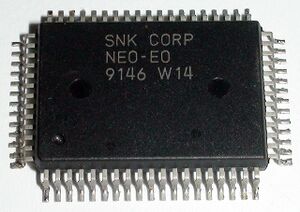
Also found in MVS systems. Probably grouped glue logic, as early AES boards had plenty of 74HC chips instead.
BIOS vector table swapping is handled by this chip. When 68k A8~A23 = 0 and the appropriate 74HC259 input (determined by memory mapped registers) is active, A22I~A23I outputs are set to 1. This makes the address appear to address decoding chips as a BIOS access instead of a P ROM access.
It also ANDs the pair of 8bit output enable signals from the NEO-C1 since there is only a single 16bit ROM used for the BIOS.
What is Y0~Y23 for? attached to memory card in AES / multislots?