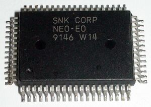
NEO-E0: Difference between revisions
Jump to navigation
Jump to search
mNo edit summary |
(Added chip position on board) |
||
| (6 intermediate revisions by one other user not shown) | |||
| Line 1: | Line 1: | ||
{{ChipInfo | |||
|picture=aes_e0.jpg | |||
|pkg=QFP64R | |||
|manu=fujitsu | |||
|date=1991 ? | |||
|gates= | |||
|used_on={{PCB|NEO-AES3-3}} ... | |||
}} | |||
= | =68k vector table swapping= | ||
The 68k vector table is swapped with the [[system ROM]] one by using {{Reg|REG_SWPBIOS}} or {{Reg|REG_SWPROM}}. | |||
A22Z~A23Z are used to make the address appear to address decoding chips as a system ROM access instead of a [[P ROM]] access. | |||
{|class="wikitable" | |||
!rowspan=2|Address||colspan=2|Maps to | |||
|- | |||
!VEC = 0||VEC = 1 | |||
|- | |||
|$000000~$0000FF||$C00000~$C000FF||$000000~$0000FF | |||
|- | |||
|$000100~$BFFFFF||colspan=2|$000100~$BFFFFF | |||
|- | |||
|$C00000~$C000FF||$000000~$0000FF||$C00000~$C000FF | |||
|- | |||
|$C00100~$FFFFFF||colspan=2|$C00100~$FFFFFF | |||
|} | |||
[[User:Kyuusaku]]: {A23Z,A22Z} = A[23:22] ^ 2{~|{A[21:7],^A[23:22],VEC}} | [[User:Kyuusaku]]: {A23Z,A22Z} = A[23:22] ^ 2{~|{A[21:7],^A[23:22],VEC}} | ||
On the AES, the AND gate is used | =Pinouts= | ||
On the AES, the AND gate is used to get /SROMOE from /SROMOEL AND /SROMOEU. | |||
==MV2B @ H7 pinout== | ==MV2B @ H7 pinout== | ||
| Line 40: | Line 65: | ||
|} | |} | ||
= | ==MV2F @ E1 pinout (to be confirmed)== | ||
{| | {| | ||
Revision as of 15:08, 6 January 2018

| |
| Package | QFP64R |
| Manufacturer | |
| First use | 1991 ? |
| Used on | NEO-AES3-3 ... |
68k vector table swapping
The 68k vector table is swapped with the system ROM one by using REG_SWPBIOS or REG_SWPROM.
A22Z~A23Z are used to make the address appear to address decoding chips as a system ROM access instead of a P ROM access.
| Address | Maps to | |
|---|---|---|
| VEC = 0 | VEC = 1 | |
| $000000~$0000FF | $C00000~$C000FF | $000000~$0000FF |
| $000100~$BFFFFF | $000100~$BFFFFF | |
| $C00000~$C000FF | $000000~$0000FF | $C00000~$C000FF |
| $C00100~$FFFFFF | $C00100~$FFFFFF | |
User:Kyuusaku: {A23Z,A22Z} = A[23:22] ^ 2{~|{A[21:7],^A[23:22],VEC}}
Pinouts
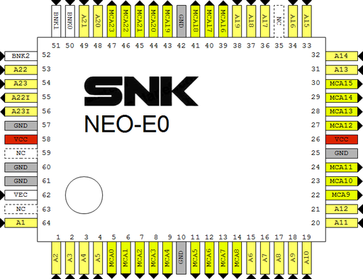
On the AES, the AND gate is used to get /SROMOE from /SROMOEL AND /SROMOEU.
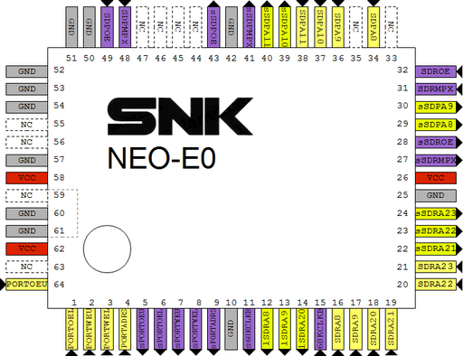
MV2B @ H7 pinout
55 = sPCK1B 56 = sPCK2B
MV2B @ G2 pinout
|
OpenOffice Draw file: File:Neo-e0 mv2b G2.odg |
|
MV2B @ F7 pinout
|
OpenOffice Draw file: File:Neo-e0 mv2b F7.odg |
Acts just as a buffer.
|
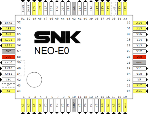
MV2F @ E1 pinout (to be confirmed)
|
OpenOffice Draw file: File:Neo-e0.odg |
|


