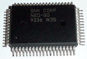
NEO-G0

| |
| Package | QFP64R |
| Manufacturer | |
| First use | 1992 ? |
| Used on | MV2B ... |
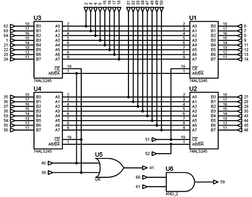
Quadruple 245 with additional OR and AND gates. Predecessor of NEO-BUF.
Internal logic
Schematic is wrong: A and B sides are flipped !
|
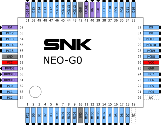
Pinouts
AES
Palette RAM and memory card access. Palette RAM /WE and P1 ROM /OE generation.
|
MV2B
-
J4: 68k data bus access for both slots. DS0,DS1: Slot 68k data enables from NEO-I0. OpenOffice Draw file: File:Neo-g0 mv2b J4.odg
-
J12: ADPCM buses access for both slots. 10 AS04: negated /ROE from YM2610, 12 AS04: negated /POE from YM2610. SLOT0, SLOT1: enables from NEO-F0. OpenOffice Draw file: File:Neo-g0 mv2b J12.odg
-
B7: Palette RAM and memory card access. Palette RAM /WE and System ROM /OE generation. 28 C0 (PAL ?):Palette RAM address decode from PRO-C0. OpenOffice Draw file: File:Neo-g0 mv2b C7.odg


