NEO-ZMC: Difference between revisions
Jump to navigation
Jump to search
m (ChipInfo) |
(Cleanup, layout and error fix about upper address lines) |
||
| Line 8: | Line 8: | ||
}} | }} | ||
{{Chipname|Z80}} '''M'''emory '''C'''ontroller. Provides a hardwired 32KiB bank and [[Z80 bankswitching|switchable 16, 8, 4, and 2KiB banks]] arranged as a register file. To save pins, the Z80's upper address lines (A15~A8) are used for data input. The chip's write strobe is [[Z80 port map|port]] address decoded inside the system. | |||
{{Chipname|Z80}} | |||
=Pinout= | =Pinout= | ||
| Line 17: | Line 15: | ||
OpenOffice Draw file: [[File:neo-zmc.odg]] | OpenOffice Draw file: [[File:neo-zmc.odg]] | ||
10, 11, 12 are | Pins 10, 11, 12 are surely not connected since the addressing scheme doesn't allow mapping over 512KiB. | ||
*SDA0,SDA1,SDA8~15: | * SDA0, SDA1, SDA8~15: Z80 address bus | ||
*SDRD0: | * SDRD0: Decoded write signal from {{Chipname|NEO-D0}} (latch on rising edge) | ||
=Operation= | =Operation= | ||
SDA8~15 is used for the bank number (data), SDA0 and SDA1 for selecting the bank zone. | |||
SDA1 | {|class="wikitable" | ||
!SDA1 | |||
!SDA0 | |||
!Z80 port | |||
!Bank zone | |||
!Address range | |||
!Size | |||
!Latch size | |||
|- | |||
|0||0||$08||0||$F000~$F7FF||2KiB||8 bits | |||
|- | |||
|0||1||$09||1||$E000~$EFFF||4KiB||7 bits | |||
|- | |||
|1||0||$0A||2||$C000~$DFFF||8KiB||6 bits | |||
|- | |||
|1||1||$0B||3||$8000~$BFFF||16KiB||5 bits | |||
|} | |||
==Details== | |||
SDRD0 must be high before configuring banks. | SDRD0 must be high before configuring banks. | ||
To configure a bank to be accessed (e.g. bank 0 in the $8000~$BFFF range): | To configure a bank to be accessed (e.g. bank 0 in the $8000~$BFFF range): | ||
*Set SDRD0 low (prepare for new bank configuration, outputs are tri-stated) | * Set SDRD0 low (prepare for new bank configuration, outputs are tri-stated) | ||
*Set SDA0~15 = '''$8003''' (select bank 0 and 16k range size) Why $8003 and not just $0003 ? | * Set SDA0~15 = '''$8003''' (select bank 0 and 16k range size) Why $8003 and not just $0003 ? | ||
*Set SDRD0 high (latch bank, ready to convert inputs to proper output signals) | * Set SDRD0 high (latch bank, ready to convert inputs to proper output signals) | ||
*Now, when the Z80 | * Now, when the Z80 reads the '''$8000~BFFF''' range, NEO-ZMC will map this to the M1 ROM zone '''$00000~$03FFF'''; | ||
To configure a bank to be accessed (e.g. bank 1 in the $8000~$BFFF range): | To configure a bank to be accessed (e.g. bank 1 in the $8000~$BFFF range): | ||
*Set SDRD0 low (prepare for new bank configuration, outputs are tri-stated) | * Set SDRD0 low (prepare for new bank configuration, outputs are tri-stated) | ||
*Set SDA0~15 = '''$8103''' (select bank 1 and 16k range size) Why $8103 and not just $0103 ? | * Set SDA0~15 = '''$8103''' (select bank 1 and 16k range size) Why $8103 and not just $0103 ? | ||
*Set SDRD0 high (latch bank, ready to convert inputs to proper output signals) | * Set SDRD0 high (latch bank, ready to convert inputs to proper output signals) | ||
*Now, when the Z80 | * Now, when the Z80 reads the '''$8000~BFFF''' range, NEO-ZMC will map this to the M1 ROM zone '''$04000~$07FFF'''; | ||
[[Category:Chips]] | [[Category:Chips]] | ||
Revision as of 03:09, 3 November 2016

| |
| Package | SOIC24 |
| Manufacturer | |
| First use | 1995 ? |
| Used on | cartridges |
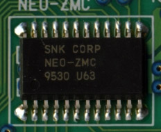
Z80 Memory Controller. Provides a hardwired 32KiB bank and switchable 16, 8, 4, and 2KiB banks arranged as a register file. To save pins, the Z80's upper address lines (A15~A8) are used for data input. The chip's write strobe is port address decoded inside the system.
Pinout
OpenOffice Draw file: File:Neo-zmc.odg
Pins 10, 11, 12 are surely not connected since the addressing scheme doesn't allow mapping over 512KiB.
- SDA0, SDA1, SDA8~15: Z80 address bus
- SDRD0: Decoded write signal from NEO-D0 (latch on rising edge)
Operation
SDA8~15 is used for the bank number (data), SDA0 and SDA1 for selecting the bank zone.
| SDA1 | SDA0 | Z80 port | Bank zone | Address range | Size | Latch size |
|---|---|---|---|---|---|---|
| 0 | 0 | $08 | 0 | $F000~$F7FF | 2KiB | 8 bits |
| 0 | 1 | $09 | 1 | $E000~$EFFF | 4KiB | 7 bits |
| 1 | 0 | $0A | 2 | $C000~$DFFF | 8KiB | 6 bits |
| 1 | 1 | $0B | 3 | $8000~$BFFF | 16KiB | 5 bits |
Details
SDRD0 must be high before configuring banks.
To configure a bank to be accessed (e.g. bank 0 in the $8000~$BFFF range):
- Set SDRD0 low (prepare for new bank configuration, outputs are tri-stated)
- Set SDA0~15 = $8003 (select bank 0 and 16k range size) Why $8003 and not just $0003 ?
- Set SDRD0 high (latch bank, ready to convert inputs to proper output signals)
- Now, when the Z80 reads the $8000~BFFF range, NEO-ZMC will map this to the M1 ROM zone $00000~$03FFF;
To configure a bank to be accessed (e.g. bank 1 in the $8000~$BFFF range):
- Set SDRD0 low (prepare for new bank configuration, outputs are tri-stated)
- Set SDA0~15 = $8103 (select bank 1 and 16k range size) Why $8103 and not just $0103 ?
- Set SDRD0 high (latch bank, ready to convert inputs to proper output signals)
- Now, when the Z80 reads the $8000~BFFF range, NEO-ZMC will map this to the M1 ROM zone $04000~$07FFF;