NEO-ZMC: Difference between revisions
Jump to navigation
Jump to search
mNo edit summary |
mNo edit summary |
||
| Line 2: | Line 2: | ||
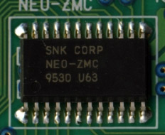
Z80 memory controller. Has a hardwired 32KiB bank and switchable 16/8/4/2KiB banks arranged as a register file. To save pins the high address lines (A15-A8) are used for data input. The chip's write strobe is (port) address decoded inside the console. | Z80 memory controller. Has a hardwired 32KiB bank and switchable 16/8/4/2KiB banks arranged as a register file. To save pins the high address lines (A15-A8) are used for data input. The chip's write strobe is (port) address decoded inside the console. | ||
(Need Z80 IN instructions details: upper 8 bytes of address bus as data, lower 8 as port number) | |||
=Pinout= | |||
[[File:Neo-zmc_pinout.png]] | |||
[[Category:Chips]] | [[Category:Chips]] | ||
Revision as of 17:11, 25 March 2011

Z80 memory controller. Has a hardwired 32KiB bank and switchable 16/8/4/2KiB banks arranged as a register file. To save pins the high address lines (A15-A8) are used for data input. The chip's write strobe is (port) address decoded inside the console.
(Need Z80 IN instructions details: upper 8 bytes of address bus as data, lower 8 as port number)