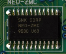
NEO-ZMC

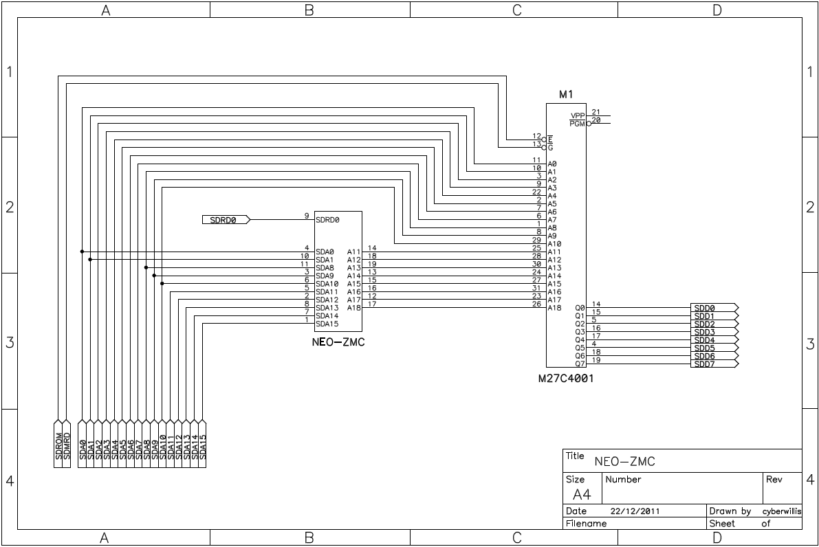
Z80 memory controller. Has a hardwired 32KiB bank and switchable 16/8/4/2KiB banks arranged as a register file. To save pins the high address lines (A15-A8) are used for data input. The chip's write strobe is (port) address decoded inside the console.
(Need Z80 IN instructions details: upper 8 bytes of address bus as data, lower 8 as port number)
Pinout
OpenOffice Draw file: File:Neo-zmc.odg
How It Work
Zmc acess the M1 in 32 banks.
Insert non-formatted text hereSDA10,SDA9,SDA8 is bank selector and SDA1,SDA0 is Rom size selector
- SDA1,SDA0 = 0,0 => 64k M1
- SDA1,SDA0 = 0,1 => 128k M1
- SDA1,SDA0 = 1,0 => 256k M1
- SDA1,SDA0 = 1,1 => 512k M1
- SDRD0 is the WRITE (configure the range and size) / READ (acess that range), selector
Example:
- PUT SDRD0 in High logic level (5v);
- PUT SDA[15..0] = $8003 (configure bank 00 + m1 512k);
- SDMRD from High to Low (this set the bank and rom size);
- SDMRD from Low to High (this fixes the bank and ZMC configure the A[18..11];
- SDMRD still in High and SDA[15..0] = $8000~$BFFF will make ZMC access M1 from $00000~$03FFF;
- Bank 00 was read
- PUT SDA[15..0] = $8103 (configure bank 01 + m1 512k);
- SDMRD from High to Low (this set the bank and rom size);
- SDMRD from Low to High (this fixes the bank and ZMC configure the A[18..11];
- SDMRD still in High and SDA[15..0] = $8000~$BFFF will make ZMC access M1 from $04000~$07FFF;
- Bank 01 was read
- PUT SDA[15..0] = $8203 (configure bank 02 + m1 512k);
- SDMRD from High to Low (this set the bank and rom size);
- SDMRD from Low to High (this fixes the bank and ZMC configure the A[18..11];
- SDMRD still in High and SDA[15..0] = $8000~$BFFF will make ZMC access M1 from $08000~$0BFFF;
- Bank 02 was read
- PUT SDA[15..0] = $8303 (configure bank 03 + m1 512k);
- SDMRD from High to Low (this set the bank and rom size);
- SDMRD from Low to High (this fixes the bank and ZMC configure the A[18..11];
- SDMRD still in High and SDA[15..0] = $8000~$BFFF will make ZMC access M1 from $0C000~$0FFFF;
- Bank 03 was read
- PUT SDA[15..0] = $8403 (configure bank 04 + m1 512k);
- SDMRD from High to Low (this set the bank and rom size);
- SDMRD from Low to High (this fixes the bank and ZMC configure the A[18..11];
- SDMRD still in High and SDA[15..0] = $8000~$BFFF will make ZMC access M1 from $10000~$13FFF;
- Bank 04 was read
... and so on...
| Here is the table for the banks of 512k rom |
|---|
| 8003 => bank 00 (acess 00000‐03FFF ); |
| 8103 => bank 01 (acess 04000‐07FFF ); |
| 8203 => bank 02 (acess 08000‐0BFFF ); |
| 8303 => bank 03 (acess 0C000‐0FFFF ); |
| 8403 => bank 04 (acess 10000‐13FFF ); |
| 8503 => bank 05 (acess 14000‐17FFF ); |
| 8603 => bank 06 (acess 18000‐1BFFF ); |
| 8703 => bank 07 (acess 1C000‐1FFFF ); |
| 8803 => bank 08 (acess 20000‐23FFF ); |
| 8903 => bank 09 (acess 24000‐27FFF ); |
| 8A03 => bank 10 (acess 28000‐2BFFF ); |
| 8B03 => bank 11 (acess 2C000‐2FFFF ); |
| 8C03 => bank 12 (acess 30000‐33FFF ); |
| 8D03 => bank 13 (acess 34000‐37FFF ); |
| 8E03 => bank 14 (acess 38000‐3BFFF ); |
| 8F03 => bank 15 (acess 3C000‐3FFFF ); |
| 9003 => bank 16 (acess 40000‐43FFF ); |
| 9103 => bank 17 (acess 40000‐47FFF ); |
| 9203 => bank 18 (acess 40000‐4BFFF ); |
| 9303 => bank 19 (acess 40000‐4FFFF ); |
| 9403 => bank 20 (acess 50000‐53FFF ); |
| 9503 => bank 21 (acess 54000‐57FFF ); |
| 9603 => bank 22 (acess 58000‐5BFFF ); |
| 9703 => bank 23 (acess 5C000‐5FFFF ); |
| 9803 => bank 24 (acess 60000‐63FFF ); |
| 9903 => bank 25 (acess 64000‐67FFF ); |
| 9A03 => bank 26 (acess 68000‐6BFFF ); |
| 9B03 => bank 27 (acess 6C000‐6FFFF ); |
| 9C03 => bank 28 (acess 70000‐73FFF ); |
| 9D03 => bank 29 (acess 74000‐77FFF ); |
| 9E03 => bank 30 (acess 78000‐7BFFF ); |
| 9F03 => bank 31 (acess 7C000‐7FFFF ); |
