|
|
| (21 intermediate revisions by 2 users not shown) |
| Line 1: |
Line 1: |
| =MVS Cartridges= | | =A/V connector= |
|
| |
|
| {| class="regdef" align="center" style="text-align:center;align:right;"
| | [[File:Av_pinout.png]] |
| |CHA bottom
| |
| |CHA top
| |
| |PROG bottom
| |
| |PROG top
| |
| |-
| |
| |[[File:mvscartchabot.png]]
| |
| |[[File:mvscartchatop.png]]
| |
| |[[File:mvscartprgbot.png]]
| |
| |[[File:mvscartprgtop.png]]
| |
| |}
| |
|
| |
|
| Signal names:
| | Note: Some home consoles revisions appear to only provide composite video, no separate sync signal. |
| *A1~A19: [[68k]] address bus
| |
| *D0~D15: 68k data bus
| |
| *R/W: 68k R/W
| |
| *AS: 68k /AS
| |
| *ROMOEL: $000000-$0FFFFF odd byte read
| |
| *ROMOEU: $000000-$0FFFFF even byte read
| |
| *ROMOE: $000000-$0FFFFF read
| |
| *PORTOEL: $200000-$2FFFFF odd byte read
| |
| *PORTOEU: $200000-$2FFFFF even byte read
| |
| *PORTWEL: $200000-$2FFFFF odd byte write
| |
| *PORTWEU: $200000-$2FFFFF even byte write
| |
| *PORTADRS: $200000-$2FFFFF any access
| |
| *SDPAD0~SDPAD7, SDRAD0~SDRAD7: [[V ROM]](s) data bus(ses) ?
| |
| *CR0~CR31: [[C ROM]]s data bus
| |
| *SDA0~SDA15: ?
| |
| *P0~P23: C ROM and [[S ROM]] address bus (multiplexed)
| |
| *PCK1B: Clock to latch C ROM address from P0~P23
| |
| *PCK2B: Clock to latch S ROM address from P0~P15
| |
| *CA4: C ROM A4
| |
| *2H1: S ROM A3
| |
| *FIXD0~FIXD7: S ROM data bus
| |
|
| |
|
| =AES Cartridges= | | =Cartridges= |
|
| |
|
| To do.
| | * [[AES cartridge pinout]] |
| | * [[MVS cartridge pinout]] |
|
| |
|
| =Joypad ports= | | =Joypad ports= |
|
| |
|
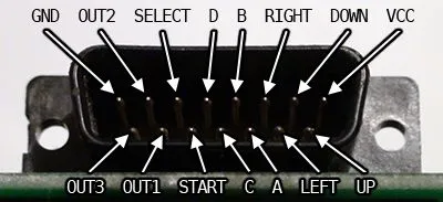
| Inputs are pulled high to +5V. | | Special, deep DA-15 connectors with a plastic shield. 10 direct inputs, 3 outputs, 2 power lines. |
| | |
| | Inputs are pulled high to +5V by [[CRE401]] R-C arrays. |
| | |
| | Outputs are open collector through 22 ohms resistors (not pulled high). |
|
| |
|
| <center>[[File:Joypad_pinout.png]]</center> | | <center>[[File:Joypad_pinout.png]]</center> |
|
| |
|
| =JAMMA connector= | | =JAMMA= |
| Infos from [[http://www.hardmvs.com HardMVS.com]]
| | |
| | See [[JAMMA connector pinout]]. |
| | |
| | =Memory card= |
| | |
| | See [[Memory card pinout]]. |
| | |
| | =MVS boards= |
| | |
| | See [[MVS board connectors pinouts]]. |
|
| |
|
| {| class="regdef"
| | =[[Multiplayer]] jack= |
| |bgcolor="#DDDDDD"|GND
| |
| |'''A'''
| |
| |'''1'''
| |
| |bgcolor="#DDDDDD"|GND
| |
| |-
| |
| |bgcolor="#DDDDDD"|GND
| |
| |'''B'''
| |
| |'''2'''
| |
| |bgcolor="#DDDDDD"|GND
| |
| |-
| |
| |bgcolor="#DD8888"| +5V
| |
| |'''C'''
| |
| |'''3'''
| |
| |bgcolor="#DD8888"| +5V
| |
| |-
| |
| |bgcolor="#DD8888"| +5V
| |
| |'''D'''
| |
| |'''4'''
| |
| |bgcolor="#DD8888"| +5V
| |
| |-
| |
| |
| |
| |'''E'''
| |
| |'''5'''
| |
| |
| |
| |-
| |
| |bgcolor="#DDDD88"| +12V
| |
| |'''F'''
| |
| |'''6'''
| |
| |bgcolor="#DDDD88"| +12V
| |
| |-
| |
| |Key
| |
| |'''H'''
| |
| |'''7'''
| |
| |Key
| |
| |-
| |
| |Coin counter #2
| |
| |'''J'''
| |
| |'''8'''
| |
| |Coin counter #1
| |
| |-
| |
| |Lockout coil #2
| |
| |'''K'''
| |
| |'''9'''
| |
| |Lockout coil #1
| |
| |-
| |
| |bgcolor="#DD8844"|Left speaker +
| |
| |'''L'''
| |
| |'''10'''
| |
| |bgcolor="#DD8844"|Right speaker +
| |
| |-
| |
| |Test switch
| |
| |'''M'''
| |
| |'''11'''
| |
| |bgcolor="#DD8844"|Mono audio +
| |
| |-
| |
| |bgcolor="#44FF44"|Video green
| |
| |'''N'''
| |
| |'''12'''
| |
| |bgcolor="#FF4444"|Video red
| |
| |-
| |
| |bgcolor="#FFFF44"|Video sync
| |
| |'''P'''
| |
| |'''13'''
| |
| |bgcolor="#4444FF"|Video blue
| |
| |-
| |
| |Service switch
| |
| |'''R'''
| |
| |'''14'''
| |
| |bgcolor="#DDDDDD"|Video GND
| |
| |-
| |
| |Coin switch #4 P2
| |
| |'''S'''
| |
| |'''15'''
| |
| |Coin switch #3 P1
| |
| |-
| |
| |Coin switch #2 P2
| |
| |'''T'''
| |
| |'''16'''
| |
| |Coin switch #1 P1
| |
| |-
| |
| |P2 Start
| |
| |'''U'''
| |
| |'''17'''
| |
| |P1 Start
| |
| |-
| |
| |P2 Up
| |
| |'''V'''
| |
| |'''18'''
| |
| |P1 Up
| |
| |-
| |
| |P2 Down
| |
| |'''W'''
| |
| |'''19'''
| |
| |P1 Down
| |
| |-
| |
| |P2 Left
| |
| |'''X'''
| |
| |'''20'''
| |
| |P1 Left
| |
| |-
| |
| |P2 Right
| |
| |'''Y'''
| |
| |'''21'''
| |
| |P1 Right
| |
| |-
| |
| |P2 A
| |
| |'''Z'''
| |
| |'''22'''
| |
| |P1 A
| |
| |-
| |
| |P2 B
| |
| |'''a'''
| |
| |'''23'''
| |
| |P1 B
| |
| |-
| |
| |P2 C
| |
| |'''b'''
| |
| |'''24'''
| |
| |P1 C
| |
| |-
| |
| |P2 D
| |
| |'''c'''
| |
| |'''25'''
| |
| |P1 D
| |
| |-
| |
| |Select down
| |
| |'''d'''
| |
| |'''26'''
| |
| |Select up
| |
| |-
| |
| |bgcolor="#DDDDDD"|GND
| |
| |'''e'''
| |
| |'''27'''
| |
| |bgcolor="#DDDDDD"|GND
| |
| |-
| |
| |bgcolor="#DDDDDD"|GND
| |
| |'''f'''
| |
| |'''28'''
| |
| |bgcolor="#DDDDDD"|GND
| |
| |}
| |
|
| |
|
| | RS-485 pair + ground. Use a stereo cable only ! |
| | |
| | * Sleeve: Ground |
| | * Ring: D- |
| | * Tip: D+ |
|
| |
|
| =CD/CDZ= | | =CD/CDZ= |
| | |
| | ==Power supply connector== |
| | |
| | [[File:Cdpow_pinout.png]] |
| | |
| | See [[power supply]]. |
|
| |
|
| ==YM2610 digital audio== | | ==YM2610 digital audio== |
| [[File:Cd2_cn7.jpg|Cd2_cn7.jpg]] | | [[File:Cd2_cn6.jpg|Cd2_cn6.jpg]] |
| Clock, L, R ?
| | |
| | # OP0 |
| | # PHI |
| | # SH2 |
| | # SH1 |
| | # Analog |
|
| |
|
| ==Video and CDDA== | | ==Video and CDDA== |
| [[File:Cd2_cn1cn3.jpg|400px]] | | [[File:Cd2_cn1cn3.jpg|400px]] |
| R, V, B, S, Burst, GND ?
| |
| Clock, L, R ?
| |
|
| |
|
| ==CD reader== | | Video: |
| | # Red |
| | # Green |
| | # Blue |
| | # Sync |
| | # Burst |
| | # GND |
| | |
| | CDDA: |
| | # LRCK |
| | # DATA |
| | # BCLK |
| | |
| | ==CD drive== |
| [[File:Cd2_cn4.jpg|400px]] | | [[File:Cd2_cn4.jpg|400px]] |
| | See [[CD drive]]. |
|
| |
|
| ==Power== | | ==PCB power== |
| [[File:Cd2_cn5.jpg]] | | [[File:Cd2_cn5.jpg]] |
|
| |
|
| =Multiplayer jack=
| | # 5V CD |
| To do.
| | # 10V CD |
| | | # 5V logic |
| | # Ground |
|
| |
|
| [[Category:Chips]] | | [[Category:Chips]] |
| [[Category:Base system]] | | [[Category:Base system]] |
A/V connector

Note: Some home consoles revisions appear to only provide composite video, no separate sync signal.
Cartridges
Joypad ports
Special, deep DA-15 connectors with a plastic shield. 10 direct inputs, 3 outputs, 2 power lines.
Inputs are pulled high to +5V by CRE401 R-C arrays.
Outputs are open collector through 22 ohms resistors (not pulled high).
JAMMA
See JAMMA connector pinout.
Memory card
See Memory card pinout.
MVS boards
See MVS board connectors pinouts.
RS-485 pair + ground. Use a stereo cable only !
- Sleeve: Ground
- Ring: D-
- Tip: D+
CD/CDZ
Power supply connector
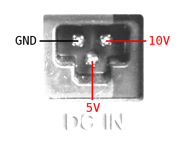
See power supply.
YM2610 digital audio
Cd2_cn6.jpg
- OP0
- PHI
- SH2
- SH1
- Analog
Video and CDDA
File:Cd2 cn1cn3.jpg
Video:
- Red
- Green
- Blue
- Sync
- Burst
- GND
CDDA:
- LRCK
- DATA
- BCLK
CD drive
File:Cd2 cn4.jpg
See CD drive.
PCB power
File:Cd2 cn5.jpg
- 5V CD
- 10V CD
- 5V logic
- Ground


