Schematics: Difference between revisions
m (→MVS (arcade)) |
m (→MVS (arcade)) |
||
| (3 intermediate revisions by 2 users not shown) | |||
| Line 17: | Line 17: | ||
</gallery> | </gallery> | ||
=MVS ( | =MVS (MV1F)= | ||
<span style="color:#FF0000"><B>Beware !</B> There's an error on page 9 (cartridge edge connections): <b>ROMOE/4MB are swapped</B>. ROMOE should be on pin 33 bottom, and 4MB is on pin 34 bottom.</span> | <span style="color:#FF0000"><B>Beware !</B> There's an error on page 9 (cartridge edge connections): <b>ROMOE/4MB are swapped</B>. ROMOE should be on pin 33 bottom, and 4MB is on pin 34 bottom.</span> | ||
| Line 23: | Line 23: | ||
<gallery widths=300px heights=190px perrow=3> | <gallery widths=300px heights=190px perrow=3> | ||
File:mv1fs-page1.jpg|'''Page 1''':{{Chipname|68k}} [[System ROM]] [[68k user RAM]] [[Battery-backed RAM]] {{Chipname|NEO-C1}} [[Joypad]] ports {{Chipname|UPD4990}} [[Battery circuit]] | File:mv1fs-page1.jpg|'''Page 1''':{{Chipname|68k}} [[System ROM]] [[68k user RAM]] [[Battery-backed RAM]] {{Chipname|NEO-C1}} [[Joypad]] ports {{Chipname|UPD4990}} [[Battery circuit]] | ||
File:mv1fs-page2.jpg|'''Page 2''':{{Chipname|LSPC2-A2}} [[VRAM]] {{Chipname|NEO-I0}} {{Chipname|NEO-B1}} {{Chipname|NEO-ZMC2}} [[SFIX]] [[L0 ROM]] | File:mv1fs-page2.jpg|'''Page 2''':{{Chipname|LSPC2-A2}} [[VRAM]] {{Chipname|NEO-I0}} {{Chipname|NEO-B1}} {{Chipname|NEO-ZMC2}} [[SFIX ROM]] [[L0 ROM]] | ||
File:mv1fs-page3.jpg|'''Page 3''':{{Chipname|NEO-E0}} [[Memory mapped registers|System latch]] [[Palette RAM]] [[Video DAC]] | File:mv1fs-page3.jpg|'''Page 3''':{{Chipname|NEO-E0}} [[Memory mapped registers|System latch]] [[Palette RAM]] [[Video DAC]] | ||
File:mv1fs-page4.jpg|'''Page 4''':{{Chipname|Z80}} [[Z80 RAM]] [[SM1]] ROM {{Chipname|NEO-D0}} {{Chipname|YM2610}} {{Chipname|YM3016}} [[Headphone amp]] | File:mv1fs-page4.jpg|'''Page 4''':{{Chipname|Z80}} [[Z80 RAM]] [[SM1]] ROM {{Chipname|NEO-D0}} {{Chipname|YM2610}} {{Chipname|YM3016}} [[Headphone amp]] | ||
| Line 32: | Line 32: | ||
File:mv1fs-page9.jpg|'''Page 9''':Cartridge connections | File:mv1fs-page9.jpg|'''Page 9''':Cartridge connections | ||
</gallery> | </gallery> | ||
=Peripheral (home/arcade)= | |||
<gallery widths=300px heights=190px perrow=3> | |||
File:Neo Geo Steering Wheel Schematic.jpg|Steering wheel schematic for Thrash Rally. | |||
</gallery> | |||
[[Category:Cartridge systems]] | [[Category:Cartridge systems]] | ||
Revision as of 04:32, 26 September 2018
AES (home)
Big thanks to Wolfsoft and ArcadeTV for the scans.
-
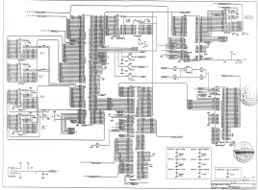
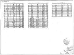
Page 1:68k 68k user RAM NEO-C1
-
Page 2:NEO-G0 Palette RAM Video DAC
-
Page 3:NEO-B1 Reset generator Joypad ports
-
-
-
-
Page 7:Video encoder
-
Page 8:cartridge slot
-
Page 9:System latch NEO-E0 Power supply
-
Page 10:Memory card
-
Page 11:Video PLL


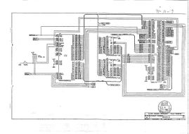
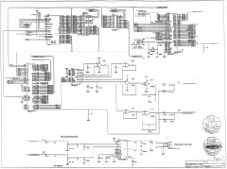
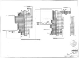
MVS (MV1F)
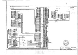
Beware ! There's an error on page 9 (cartridge edge connections): ROMOE/4MB are swapped. ROMOE should be on pin 33 bottom, and 4MB is on pin 34 bottom.
-
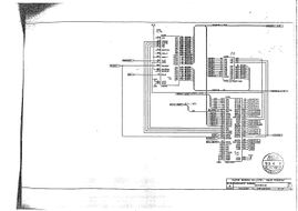
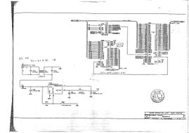
Page 1:68k System ROM 68k user RAM Battery-backed RAM NEO-C1 Joypad ports UPD4990 Battery circuit
-
-
Page 3:NEO-E0 System latch Palette RAM Video DAC
-
-

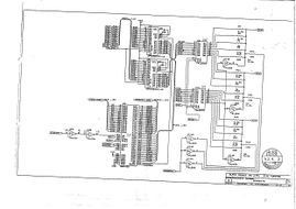
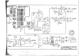
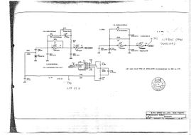
Page 5:Power amp NEO-F0 DIP switches Cab interface
-
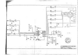
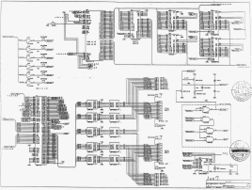
Page 6:Daughterboard connections
-
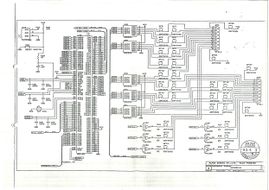
Page 7
-
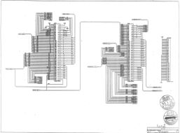
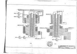
Page 8:Daughterboard connections
-
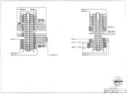
Page 9:Cartridge connections


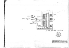
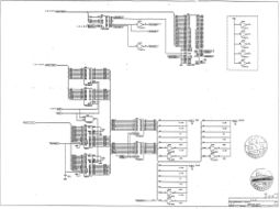
Peripheral (home/arcade)
-
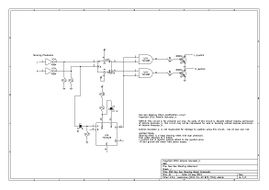
Steering wheel schematic for Thrash Rally.
