NEO-SMA: Difference between revisions
m (1 revision) |
m (Added "used on" board) |
||
| (10 intermediate revisions by 4 users not shown) | |||
| Line 1: | Line 1: | ||
{{ChipInfo | |||
|picture=crt_sma.jpg | |||
|pkg=QFP144 | |||
|manu=Seiko Epson | |||
|date=1999 ? | |||
|gates=? | |||
|used_on={{PCB|PROGLBA}} {{PCB|PROGSMA}} | |||
}} | |||
Info from [[https://github.com/mamedev/mame/blob/master/src/devices/bus/neogeo/sma.cpp MAME's source]] | |||
Security chip found connected to the [[P ROM]]s in [[The King of Fighters '99 - Millennium Battle]] (not all sets), [[The King of Fighters 2000]] (not all sets), [[Metal Slug 3]] (not all sets) and in [[Garou - Mark of the Wolves]] (all sets) [[cartridges]]. Bankswitches the [[68k memory map|second megabyte]] ($200000~$2FFFFF) of P ROM space and provides a 16bit pseudo-random number generator. | |||
Upon system reset, the PRN is initialized to $2345. | |||
The chip always (?) replies $9A37 on reads. | |||
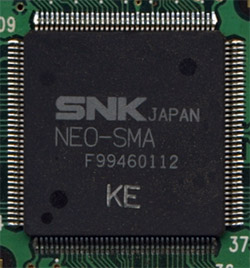
The stamp marking suggests that it is a programmable chip (OTP ?). | |||
=Pinout= | |||
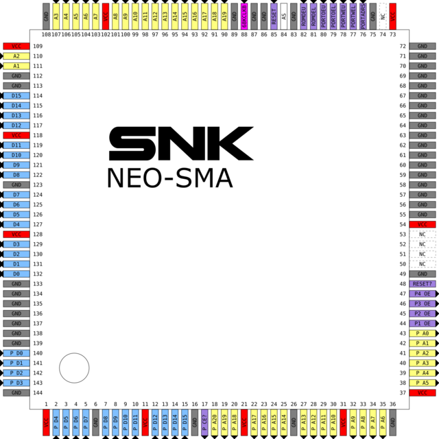
{{Pinout|NEO-SMA|640}} | |||
Pin list by [[User:hpman]]. | |||
=PRNG= | |||
16bit LSFR with taps at bits 2, 3, 5, 6, 7, 11, 12, 15. Each read steps the register. | |||
[[File:Smalfsr.png]] | |||
=Bankswitching= | |||
Bankswitching is done by unscrambling the written bank number and using a 64 entry (256 bytes) lookup table to map the P ROM into $200000~$2FFFFF. | |||
==KOF 99== | |||
[[File:Smabskof99.png|300px|thumb]] | |||
*Bankswitching write at $2FFFF1 | |||
*Read chip presence at $2FE447 | |||
*PRN at $2FFFF8 and $2FFFFA | |||
Bankswitch LUT (P2 ROM address): | |||
{|class="wikitable" | |||
! !!0!!1!!2!!3!!4!!5!!6!!7!!8!!9!!A!!B!!C!!D!!E!!F | |||
|- | |||
!0 | |||
|$000000||$100000||$200000||$300000||$3CC000||$4CC000||$3F2000||$4F2000||$407800||$507800||$40D000||$50D000||$417800||$517800||$420800||$520800 | |||
|- | |||
!1 | |||
|$424800||$524800||$429000||$529000||$42E800||$52E800||$431800||$531800||$54D000||$551000||$567000||$592800||$588800||$581800||$599800||$594800 | |||
|- | |||
!2 | |||
|$598000||?||?||?||?||?||?||?||?||?||?||?||?||?||?||? | |||
|- | |||
!3 | |||
|?||?||?||?||?||?||?||?||?||?||?||?||?||?||?||? | |||
|} | |||
==Garou== | |||
*Bankswitching write at $2FFFC0 | |||
*Read chip presence at $2FE447 | |||
*PRN at $2FFFCC and $2FFFF0 | |||
"KF" chip revision: | |||
Bank scambling=12,14,6,7,9,5 | |||
{|class="wikitable" | |||
! !!0!!1!!2!!3!!4!!5!!6!!7!!8!!9!!A!!B!!C!!D!!E!!F | |||
|- | |||
!0 | |||
|$000000||$100000||$200000||$300000||$280000||$380000||$2D0000||$3D0000||$2F0000||$3F0000||$400000||$500000||$420000||$520000||$440000||$540000 | |||
|- | |||
!1 | |||
|$498000||$598000||$4A0000||$5A0000||$4A8000||$5A8000||$4B0000||$5B0000||$4B8000||$5B8000||$4C0000||$5C0000||$4C8000||$5C8000||$4D0000||$5D0000 | |||
|- | |||
!2 | |||
|$458000||$558000||$460000||$560000||$468000||$568000||$470000||$570000||$478000||$578000||$480000||$580000||$488000||$588000||$490000||$590000 | |||
|- | |||
!3 | |||
|$5D0000||$5D8000||$5E0000||$5E8000||$5F0000||$5F8000||$600000||?||?||?||?||?||?||?||?||? | |||
|} | |||
"KE" chip revision: | |||
Bank scambling=13,11,2,14,8,4 | |||
{|class="wikitable" | |||
! !!0!!1!!2!!3!!4!!5!!6!!7!!8!!9!!A!!B!!C!!D!!E!!F | |||
|- | |||
!0 | |||
|$000000||$100000||$200000||$300000||$280000||$380000||$2D0000||$3D0000||$2C8000||$3C8000||$400000||$500000||$420000||$520000||$440000||$540000 | |||
|- | |||
!1 | |||
|$598000||$698000||$5A0000||$6A0000||$5A8000||$6A8000||$5B0000||$6B0000||$5B8000||$6B8000||$5C0000||$6C0000||$5C8000||$6C8000||$5D0000||$6D0000 | |||
|- | |||
!2 | |||
|$458000||$558000||$460000||$560000||$468000||$568000||$470000||$570000||$478000||$578000||$480000||$580000||$488000||$588000||$490000||$590000 | |||
|- | |||
!3 | |||
|$5D8000||$6D8000||$5E0000||$6E0000||$5E8000||$6E8000||$6E8000||$000000||$000000||$000000||$000000||$000000||$000000||$000000||$000000||$000000 | |||
|} | |||
==Metal Slug 3== | |||
[[File:Smabsms3.png|300px|thumb]] | |||
*Bankswitching write at $2FFFE5 | |||
*Read chip presence at $2FE447 | |||
*PRN at $2FFFF8 and $2FFFFA | |||
Bankswitch LUT (P2 ROM address): | |||
{|class="wikitable" | |||
! !!0!!1!!2!!3!!4!!5!!6!!7!!8!!9!!A!!B!!C!!D!!E!!F | |||
|- | |||
!0 | |||
|$000000||$020000||$040000||$060000||$070000||$090000||$0B0000||$0D0000||$0E0000||$0F0000||$120000||$130000||$140000||$150000||$180000||$190000 | |||
|- | |||
!1 | |||
|$1A0000||$1B0000||$1E0000||$1F0000||$200000||$210000||$240000||$250000||$260000||$270000||$2A0000||$2B0000||$2C0000||$2D0000||$300000||$310000 | |||
|- | |||
!2 | |||
|$320000||$330000||$360000||$370000||$380000||$390000||$3C0000||$3D0000||$400000||$410000||$440000||$450000||$460000||$470000||$4A0000||$4B0000 | |||
|- | |||
!3 | |||
|$4C0000||?||?||?||?||?||?||?||?||?||?||?||?||?||?||? | |||
|} | |||
==KOF 2000== | |||
[[File:Smabskof2k.png|300px|thumb]] | |||
*Bankswitching write at $2FFFED | |||
*Read chip presence at $2FE447 | |||
*PRN at $2FFFD8 and $2FFFDA | |||
Bankswitch LUT (P2 ROM address): | |||
{|class="wikitable" | |||
! !!0!!1!!2!!3!!4!!5!!6!!7!!8!!9!!A!!B!!C!!D!!E!!F | |||
|- | |||
!0 | |||
|$000000||$100000||$200000||$300000||$3F7800||$4F7800||$3FF800||$4FF800||$407800||$507800||$40F800||$50F800||$416800||$516800||$41D800||$51D800 | |||
|- | |||
!1 | |||
|$424000||$524000||$523800||$623800||$526000||$626000||$528000||$628000||$52A000||$62A000||$52B800||$62B800||$52D000||$62D000||$52E800||$62E800 | |||
|- | |||
!2 | |||
|$618000||$619000||$61A000||$61A800||?||?||?||?||?||?||?||?||?||?||?||? | |||
|- | |||
!3 | |||
|?||?||?||?||?||?||?||?||?||?||?||?||?||?||?||? | |||
|} | |||
[[Category:Chips]] | [[Category:Chips]] | ||
Latest revision as of 11:34, 17 February 2022
| |
| Package | QFP144 |
| Manufacturer | File:Logo Seiko Epson.jpg |
| First use | 1999 ? |
| Used on | PROGLBA PROGSMA |
Info from [MAME's source]
Security chip found connected to the P ROMs in The King of Fighters '99 - Millennium Battle (not all sets), The King of Fighters 2000 (not all sets), Metal Slug 3 (not all sets) and in Garou - Mark of the Wolves (all sets) cartridges. Bankswitches the second megabyte ($200000~$2FFFFF) of P ROM space and provides a 16bit pseudo-random number generator.
Upon system reset, the PRN is initialized to $2345.
The chip always (?) replies $9A37 on reads.
The stamp marking suggests that it is a programmable chip (OTP ?).
Pinout
Pin list by User:hpman.
PRNG
16bit LSFR with taps at bits 2, 3, 5, 6, 7, 11, 12, 15. Each read steps the register.
Bankswitching
Bankswitching is done by unscrambling the written bank number and using a 64 entry (256 bytes) lookup table to map the P ROM into $200000~$2FFFFF.
KOF 99
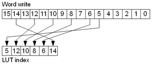
- Bankswitching write at $2FFFF1
- Read chip presence at $2FE447
- PRN at $2FFFF8 and $2FFFFA
Bankswitch LUT (P2 ROM address):
| 0 | 1 | 2 | 3 | 4 | 5 | 6 | 7 | 8 | 9 | A | B | C | D | E | F | |
|---|---|---|---|---|---|---|---|---|---|---|---|---|---|---|---|---|
| 0 | $000000 | $100000 | $200000 | $300000 | $3CC000 | $4CC000 | $3F2000 | $4F2000 | $407800 | $507800 | $40D000 | $50D000 | $417800 | $517800 | $420800 | $520800 |
| 1 | $424800 | $524800 | $429000 | $529000 | $42E800 | $52E800 | $431800 | $531800 | $54D000 | $551000 | $567000 | $592800 | $588800 | $581800 | $599800 | $594800 |
| 2 | $598000 | ? | ? | ? | ? | ? | ? | ? | ? | ? | ? | ? | ? | ? | ? | ? |
| 3 | ? | ? | ? | ? | ? | ? | ? | ? | ? | ? | ? | ? | ? | ? | ? | ? |
Garou
- Bankswitching write at $2FFFC0
- Read chip presence at $2FE447
- PRN at $2FFFCC and $2FFFF0
"KF" chip revision:
Bank scambling=12,14,6,7,9,5
| 0 | 1 | 2 | 3 | 4 | 5 | 6 | 7 | 8 | 9 | A | B | C | D | E | F | |
|---|---|---|---|---|---|---|---|---|---|---|---|---|---|---|---|---|
| 0 | $000000 | $100000 | $200000 | $300000 | $280000 | $380000 | $2D0000 | $3D0000 | $2F0000 | $3F0000 | $400000 | $500000 | $420000 | $520000 | $440000 | $540000 |
| 1 | $498000 | $598000 | $4A0000 | $5A0000 | $4A8000 | $5A8000 | $4B0000 | $5B0000 | $4B8000 | $5B8000 | $4C0000 | $5C0000 | $4C8000 | $5C8000 | $4D0000 | $5D0000 |
| 2 | $458000 | $558000 | $460000 | $560000 | $468000 | $568000 | $470000 | $570000 | $478000 | $578000 | $480000 | $580000 | $488000 | $588000 | $490000 | $590000 |
| 3 | $5D0000 | $5D8000 | $5E0000 | $5E8000 | $5F0000 | $5F8000 | $600000 | ? | ? | ? | ? | ? | ? | ? | ? | ? |
"KE" chip revision:
Bank scambling=13,11,2,14,8,4
| 0 | 1 | 2 | 3 | 4 | 5 | 6 | 7 | 8 | 9 | A | B | C | D | E | F | |
|---|---|---|---|---|---|---|---|---|---|---|---|---|---|---|---|---|
| 0 | $000000 | $100000 | $200000 | $300000 | $280000 | $380000 | $2D0000 | $3D0000 | $2C8000 | $3C8000 | $400000 | $500000 | $420000 | $520000 | $440000 | $540000 |
| 1 | $598000 | $698000 | $5A0000 | $6A0000 | $5A8000 | $6A8000 | $5B0000 | $6B0000 | $5B8000 | $6B8000 | $5C0000 | $6C0000 | $5C8000 | $6C8000 | $5D0000 | $6D0000 |
| 2 | $458000 | $558000 | $460000 | $560000 | $468000 | $568000 | $470000 | $570000 | $478000 | $578000 | $480000 | $580000 | $488000 | $588000 | $490000 | $590000 |
| 3 | $5D8000 | $6D8000 | $5E0000 | $6E0000 | $5E8000 | $6E8000 | $6E8000 | $000000 | $000000 | $000000 | $000000 | $000000 | $000000 | $000000 | $000000 | $000000 |
Metal Slug 3
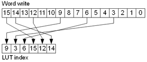
- Bankswitching write at $2FFFE5
- Read chip presence at $2FE447
- PRN at $2FFFF8 and $2FFFFA
Bankswitch LUT (P2 ROM address):
| 0 | 1 | 2 | 3 | 4 | 5 | 6 | 7 | 8 | 9 | A | B | C | D | E | F | |
|---|---|---|---|---|---|---|---|---|---|---|---|---|---|---|---|---|
| 0 | $000000 | $020000 | $040000 | $060000 | $070000 | $090000 | $0B0000 | $0D0000 | $0E0000 | $0F0000 | $120000 | $130000 | $140000 | $150000 | $180000 | $190000 |
| 1 | $1A0000 | $1B0000 | $1E0000 | $1F0000 | $200000 | $210000 | $240000 | $250000 | $260000 | $270000 | $2A0000 | $2B0000 | $2C0000 | $2D0000 | $300000 | $310000 |
| 2 | $320000 | $330000 | $360000 | $370000 | $380000 | $390000 | $3C0000 | $3D0000 | $400000 | $410000 | $440000 | $450000 | $460000 | $470000 | $4A0000 | $4B0000 |
| 3 | $4C0000 | ? | ? | ? | ? | ? | ? | ? | ? | ? | ? | ? | ? | ? | ? | ? |
KOF 2000
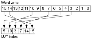
- Bankswitching write at $2FFFED
- Read chip presence at $2FE447
- PRN at $2FFFD8 and $2FFFDA
Bankswitch LUT (P2 ROM address):
| 0 | 1 | 2 | 3 | 4 | 5 | 6 | 7 | 8 | 9 | A | B | C | D | E | F | |
|---|---|---|---|---|---|---|---|---|---|---|---|---|---|---|---|---|
| 0 | $000000 | $100000 | $200000 | $300000 | $3F7800 | $4F7800 | $3FF800 | $4FF800 | $407800 | $507800 | $40F800 | $50F800 | $416800 | $516800 | $41D800 | $51D800 |
| 1 | $424000 | $524000 | $523800 | $623800 | $526000 | $626000 | $528000 | $628000 | $52A000 | $62A000 | $52B800 | $62B800 | $52D000 | $62D000 | $52E800 | $62E800 |
| 2 | $618000 | $619000 | $61A000 | $61A800 | ? | ? | ? | ? | ? | ? | ? | ? | ? | ? | ? | ? |
| 3 | ? | ? | ? | ? | ? | ? | ? | ? | ? | ? | ? | ? | ? | ? | ? | ? |
