NEO-MGA: Difference between revisions
Jump to navigation
Jump to search
mNo edit summary |
m (→CD pinout) |
||
| (7 intermediate revisions by the same user not shown) | |||
| Line 1: | Line 1: | ||
{{ChipInfo | |||
|picture=cd1_neo-mga.jpg | |||
|pkg=QFP160 | |||
|manu=fujitsu | |||
|date=1994 ? | |||
|gates=? | |||
|used_on={{PCB|CDROM-2 board|CDROM-2}}, {{PCB|MV1A}}... | |||
}} | |||
Multi-purpose chip found in CD systems and some late MVS boards: | |||
* NEO-MGA in the CD1 model (front loading). | * NEO-MGA in the CD1 model (front loading). | ||
* NEO-MGA-T in the CD2 model (top loading) and | * {{Chipname|NEO-MGA-T}} in the CD2 model (top loading) and {{PCB|MV1A}} MVS boards, can be swapped with NEO-MGA. | ||
* NEO- | * {{Chipname|NEO-MGA2-SA}} in the [[CDZ]], replaces the {{Chipname|LC8953}} ? | ||
It is used for address decoding, communication with the [[CD drive]], for refreshing {{Chipname|68k}} [[DRAM]], and for buffering serial [[CDDA]] data. | |||
=CD pinout= | |||
Pin 93: GND ! | |||
[[File:Neo-mga_CD_pinout.png|700px]] | |||
[[File:Neo-mga_cd.odg]] | |||
=MV1A pinout= | |||
[[File:Neo-mga_MV1A_pinout.png|700px]] | |||
[[File:Neo- | [[File:Neo-mga_mv1a.odg]] | ||
= | =Signals= | ||
* DRM*, RAS, CAS, WRITE: See TC514400 DRAM datasheet. | |||
* X*: See [[LC8953]] datasheet. | |||
[[Category:Chips]] | [[Category:Chips]] | ||
Latest revision as of 23:22, 20 September 2022
| File:Cd1 neo-mga.jpg | |
| Package | QFP160 |
| Manufacturer | |
| First use | 1994 ? |
| Used on | CDROM-2 board, MV1A... |
Multi-purpose chip found in CD systems and some late MVS boards:
- NEO-MGA in the CD1 model (front loading).
- NEO-MGA-T in the CD2 model (top loading) and MV1A MVS boards, can be swapped with NEO-MGA.
- NEO-MGA2-SA in the CDZ, replaces the LC8953 ?
It is used for address decoding, communication with the CD drive, for refreshing 68k DRAM, and for buffering serial CDDA data.
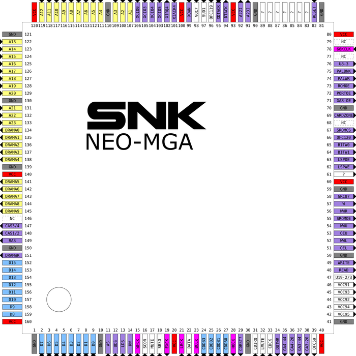
CD pinout
Pin 93: GND !
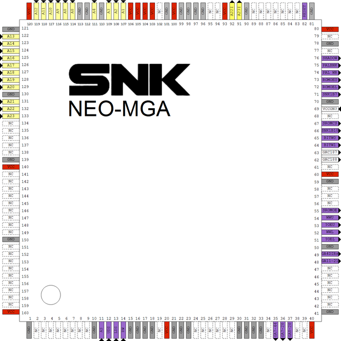
MV1A pinout
Signals
- DRM*, RAS, CAS, WRITE: See TC514400 DRAM datasheet.
- X*: See LC8953 datasheet.

