SLOT6 board: Difference between revisions
Jump to navigation
Jump to search
(Created page with "400px|right File:Slot6_details.jpg ==Chip 1: 74F244 Upper 68k address lines== File:Slot6_chip1.png ==Chip 2: 74LS244 Middle 68k address l...") |
No edit summary |
||
| (4 intermediate revisions by 2 users not shown) | |||
| Line 2: | Line 2: | ||
[[File:Slot6_details.jpg]] | [[File:Slot6_details.jpg]] | ||
==Chip 1: 74F244 | [[File:74151.png]] | ||
=C ROM data= | |||
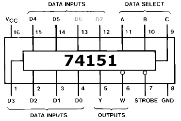
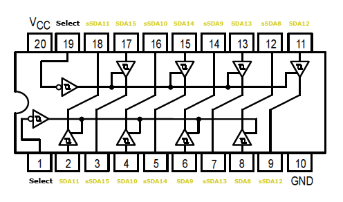
CR0~CR31 are multiplexed by 32 74LS251 8-to-1 data selectors. See [[Graphic glitches]]. | |||
*K28: CR0 | |||
*K29: CR1 | |||
*K30: CR2 | |||
*J28: CR3 | |||
*J29: CR4 | |||
*J30: CR5 | |||
*H28: CR6 | |||
*H29: CR7 | |||
*H30: CR8 | |||
*G28: CR9 | |||
*G29: CR10 | |||
*G30: CR11 | |||
*F28: CR12 | |||
*F29: CR13 | |||
*F30: CR14 | |||
*E28: CR15 | |||
*E29: CR16 | |||
*E30: CR17 | |||
*D28: CR18 | |||
*D29: CR19 | |||
*K3: CR20 | |||
*K2: CR21 | |||
*J3: CR22 | |||
*J2: CR23 | |||
*H3: CR24 | |||
*H2: CR25 | |||
*G3: CR26 | |||
*G2: CR27 | |||
*G1: CR82 | |||
*F3: CR29 | |||
*F2: CR30 | |||
*F1: CR31 | |||
=S ROM data= | |||
FIXD0~FIXD7 are multiplexed by 8 74LS251 8-to-1 data selectors. See [[Graphic glitches]]. | |||
*E3: FIXD0 | |||
*E2: FIXD1 | |||
*D3: FIXD2 | |||
*D2: FIXD3 | |||
*D1: FIXD4 | |||
*C3: FIXD5 | |||
*C2: FIXD6 | |||
*C1: FIXD7 | |||
=Blocks= | |||
==Chip 1, 2 & 3: 74F244 [[68k]] address lines== | |||
[[File:Slot6_chip1.png]] | [[File:Slot6_chip1.png]] | ||
[[File:Slot6_chip2.png]] | [[File:Slot6_chip2.png]] | ||
[[File:Slot6_chip3.png]] | [[File:Slot6_chip3.png]] | ||
| Line 14: | Line 65: | ||
[[File:Slot6_chip4.png]] | [[File:Slot6_chip4.png]] | ||
==Chip 5: 74LS245 | ==Chip 5 & 6: 74LS245 68k data lines== | ||
[[File:Slot6_chip5.png]] | [[File:Slot6_chip5.png]] | ||
[[File:Slot6_chip6.png]] | [[File:Slot6_chip6.png]] | ||
==Chip 7: 74LS244 | ==Chip 7 & 8: 74LS244 P odd lines and clocks== | ||
[[File:Slot6_chip7.png]] | [[File:Slot6_chip7.png]] | ||
[[File:Slot6_chip8.png]] | [[File:Slot6_chip8.png]] | ||
==Chip 9: 74LS245 | ==Chip 9 & 10: 74LS245 P even lines, C/S address, P clocks== | ||
[[File:Slot6_chip9.png]] | [[File:Slot6_chip9.png]] | ||
[[File:Slot6_chip10.png]] | [[File:Slot6_chip10.png]] | ||
==Chip 11: 74LS245 PCM-A ROM multiplexed bus 0~ | ==Chip 11 & 13: 74LS245 PCM-A ROM multiplexed bus 0~23== | ||
[[File:Slot6_chip11.png]] | [[File:Slot6_chip11.png]] | ||
[[File:Slot6_chip13.png]] | |||
==Chip 12: 74LS245 PCM-B ROM multiplexed bus 0~ | Note: it looks like SDRADx and sSDRADx are swapped on chip 11 schematic compared to real board. | ||
==Chip 12 & 14: 74LS245 PCM-B ROM multiplexed bus 0~11== | |||
[[File:Slot6_chip12.png]] | [[File:Slot6_chip12.png]] | ||
[[File:Slot6_chip14.png]] | |||
Note: it looks like SDRADx and sSDRADx are swapped on chip 12 schematic compared to real board. | |||
==Chip 15: 74LS245 [[Z80]] D0~D7== | ==Chip 15: 74LS245 [[Z80]] D0~D7== | ||
| Line 50: | Line 95: | ||
[[File:Slot6_chip16.png]] | [[File:Slot6_chip16.png]] | ||
==Chip 17: 74LS244 | ==Chip 17 & 18: 74LS244 Z80 address lines== | ||
[[File:Slot6_chip17.png]] | [[File:Slot6_chip17.png]] | ||
[[File:Slot6_chip18.png]] | [[File:Slot6_chip18.png]] | ||
[[Category:Repairs]] | [[Category:Repairs]] | ||
[[Category:Cartridge systems]] | |||
Latest revision as of 20:59, 23 June 2024
C ROM data
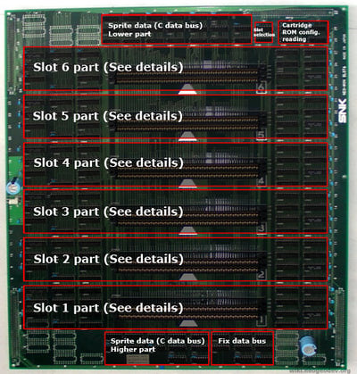
CR0~CR31 are multiplexed by 32 74LS251 8-to-1 data selectors. See Graphic glitches.
- K28: CR0
- K29: CR1
- K30: CR2
- J28: CR3
- J29: CR4
- J30: CR5
- H28: CR6
- H29: CR7
- H30: CR8
- G28: CR9
- G29: CR10
- G30: CR11
- F28: CR12
- F29: CR13
- F30: CR14
- E28: CR15
- E29: CR16
- E30: CR17
- D28: CR18
- D29: CR19
- K3: CR20
- K2: CR21
- J3: CR22
- J2: CR23
- H3: CR24
- H2: CR25
- G3: CR26
- G2: CR27
- G1: CR82
- F3: CR29
- F2: CR30
- F1: CR31
S ROM data
FIXD0~FIXD7 are multiplexed by 8 74LS251 8-to-1 data selectors. See Graphic glitches.
- E3: FIXD0
- E2: FIXD1
- D3: FIXD2
- D2: FIXD3
- D1: FIXD4
- C3: FIXD5
- C2: FIXD6
- C1: FIXD7
Blocks
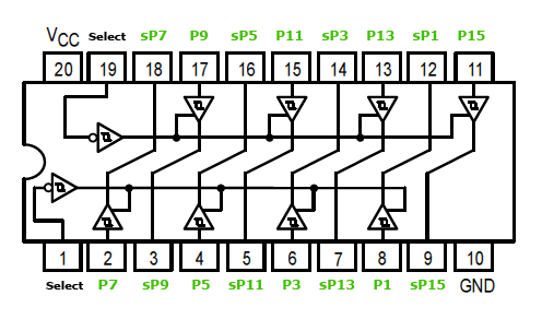
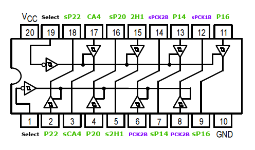
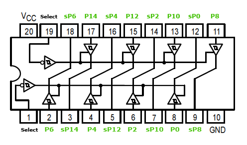
Chip 1, 2 & 3: 74F244 68k address lines
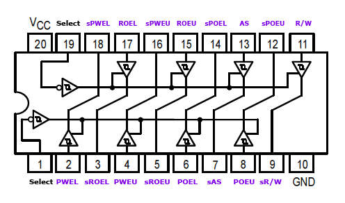
Chip 4: 74LS244 68k ROMs control lines
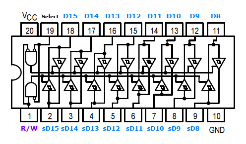
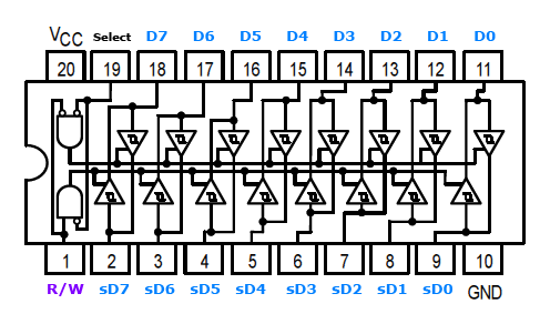
Chip 5 & 6: 74LS245 68k data lines
Chip 7 & 8: 74LS244 P odd lines and clocks
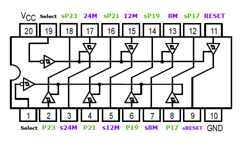
Chip 9 & 10: 74LS245 P even lines, C/S address, P clocks
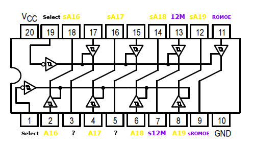
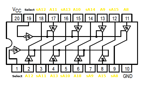
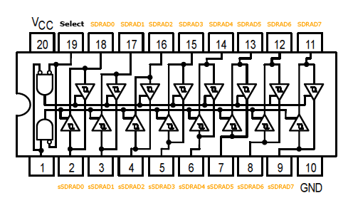
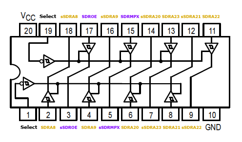
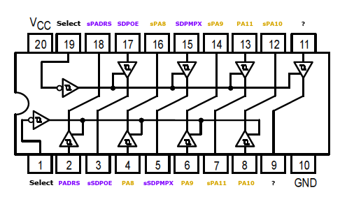
Chip 11 & 13: 74LS245 PCM-A ROM multiplexed bus 0~23
Note: it looks like SDRADx and sSDRADx are swapped on chip 11 schematic compared to real board.
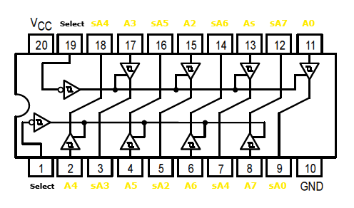
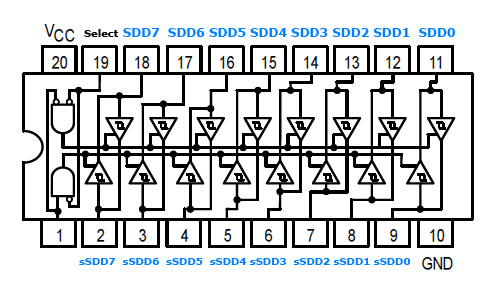
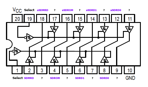
Chip 12 & 14: 74LS245 PCM-B ROM multiplexed bus 0~11
Note: it looks like SDRADx and sSDRADx are swapped on chip 12 schematic compared to real board.

