PCM: Difference between revisions
mNo edit summary |
(Changed 1st use from 1992 ? to 1990 (source : https://www.mvs-scans.com/index.php/File:Eight_man_set1_b1_front.jpg )) |
||
| (12 intermediate revisions by 2 users not shown) | |||
| Line 1: | Line 1: | ||
{{ChipInfo | |||
|picture=crt_pcm.jpg | |||
|pkg=QFP80R | |||
|manu=fujitsu | |||
|date=1990 | |||
|gates= | |||
|used_on=[[Cartridges]] | |||
}} | |||
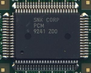
PCM (not "'''NEO'''-PCM" probably because it was used in some SNK claw cranes) is a {{Chipname|V ROM}} banking and demultiplexing chip, found in AES and MVS [[cartridges]], and on [[ROM-Only boards|ROM-only]] arcade boards. | |||
[[ | Early cartridges had separate [[YM2610|ADPCM]]-A and ADPCM-B sound ROMs. Since one was often emptier than the other, SNK devised a way to mix both types in the same ROM chip to save space and reduce costs. | ||
On some [[cartridge | {{Chipname|NEO-PCM2}} can also be found in late cartridges, and with {{Chipname|NEO-YSA2}}. | ||
On some [[:Category:cartridge boards|Cartridge boards]], VA20~VA22 are used to select which of the 4 possible V ROMs to use (decoded by a LS139). | |||
Uses several latches for address and data, as well as a counter clocked by {{Sig|68KCLKB|68KCLKB}} for synchronisation. | |||
=Internal logic= | =Internal logic= | ||
The trick takes advantage of the asynchronous and predictable access to the ADPCM-A and APDCM-B data by the {{Chipname|YM2610}}. See [[YM2610 bus timing]]. | |||
Verilog | [[https://github.com/neogeodev/SNKVerilog/tree/master/PCM Verilog definition]]. | ||
=Pinout= | =Pinout= | ||
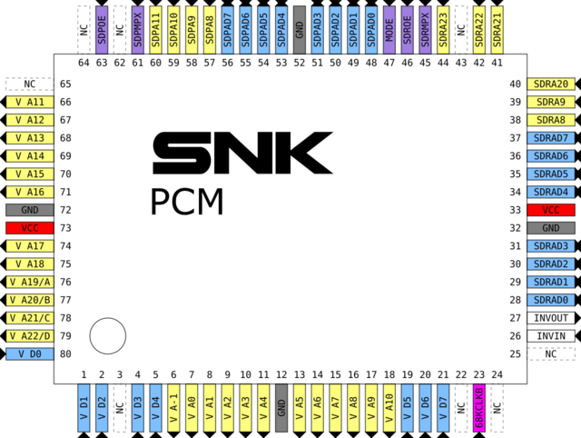
{{Pinout|PCM|640}} | |||
*INVIN, INVOUT: Simple inverter | |||
*SDPOE, SDROE, SDPMPX, SDRMPX: from the | *SDPOE, SDROE, SDPMPX, SDRMPX: from the YM2610 | ||
*SDRAD0~SDRAD7: ADPCM-A multiplexed bus part | *SDRAD0~SDRAD7: ADPCM-A multiplexed bus part | ||
*SDPAD0~SDPAD7: ADPCM-B multiplexed bus part | *SDPAD0~SDPAD7: ADPCM-B multiplexed bus part | ||
*SDRA8,SDRA9,SDRA20~SDRA23: ADPCM-A address bus | *SDRA8, SDRA9, SDRA20~SDRA23: ADPCM-A address bus | ||
*SDPA8~SDPA11: ADPCM-B address bus | *SDPA8~SDPA11: ADPCM-B address bus | ||
*V D0~V D7: V ROM(s) data bus | *V D0~V D7: V ROM(s) data bus | ||
*V | *V A-1~V A22: V ROM(s) address bus | ||
** When the MODE pin is low, V A19~V A22 become 4 active-low decoded outputs (based on value from the internal V A19 and V A20). | |||
[[Category:Chips]] | [[Category:Chips]] | ||
Latest revision as of 18:13, 11 December 2025

| |
| Package | QFP80R |
| Manufacturer | |
| First use | 1990 |
| Used on | Cartridges |
PCM (not "NEO-PCM" probably because it was used in some SNK claw cranes) is a V ROM banking and demultiplexing chip, found in AES and MVS cartridges, and on ROM-only arcade boards.
Early cartridges had separate ADPCM-A and ADPCM-B sound ROMs. Since one was often emptier than the other, SNK devised a way to mix both types in the same ROM chip to save space and reduce costs.
NEO-PCM2 can also be found in late cartridges, and with NEO-YSA2.
On some Cartridge boards, VA20~VA22 are used to select which of the 4 possible V ROMs to use (decoded by a LS139).
Uses several latches for address and data, as well as a counter clocked by 68KCLKB for synchronisation.
Internal logic
The trick takes advantage of the asynchronous and predictable access to the ADPCM-A and APDCM-B data by the YM2610. See YM2610 bus timing.
Pinout
- INVIN, INVOUT: Simple inverter
- SDPOE, SDROE, SDPMPX, SDRMPX: from the YM2610
- SDRAD0~SDRAD7: ADPCM-A multiplexed bus part
- SDPAD0~SDPAD7: ADPCM-B multiplexed bus part
- SDRA8, SDRA9, SDRA20~SDRA23: ADPCM-A address bus
- SDPA8~SDPA11: ADPCM-B address bus
- V D0~V D7: V ROM(s) data bus
- V A-1~V A22: V ROM(s) address bus
- When the MODE pin is low, V A19~V A22 become 4 active-low decoded outputs (based on value from the internal V A19 and V A20).
