NEO-ZMC: Difference between revisions
Jump to navigation
Jump to search
mNo edit summary |
(Error in date, found an older chip) |
||
| (41 intermediate revisions by 5 users not shown) | |||
| Line 1: | Line 1: | ||
{{ChipInfo | |||
|picture=crt_zmc.jpg | |||
|pkg=SOIC24 | |||
|manu=fujitsu | |||
|date=1991 ? | |||
|gates= | |||
|used_on=[[cartridges]] | |||
}} | |||
{{Chipname|Z80}} '''M'''emory '''C'''ontroller. Handles the [[Z80]] bankswitching in cartridges. To save pins, the Z80's upper address line are also used as data input. The chip's write strobe SDRD0 is [[Z80 port map|port]] address decoded inside the system. | |||
[[ | =Pinout= | ||
{{Pinout|NEO-ZMC|512}} | |||
Pins 10, 11, 12 may be M1 higher address bits ? | |||
* SDA0, SDA1, SDA8~15: Z80 address bus | |||
* M1 A11~M1 A18: [[M1 ROM]] address lines | |||
* SDRD0: Decoded write signal from {{Chipname|NEO-D0}} (latch on rising edge) | |||
=Operation= | |||
SDA8~SDA15 are used for the bank number (data), SDA0 and SDA1 for selecting the window. | |||
{|class="wikitable" | |||
!SDA1 | |||
!SDA0 | |||
!Z80 port | |||
!Window | |||
!Address range | |||
!Size | |||
!Latch size | |||
|- | |||
|0||0||$08||0||$F000~$F7FF||2KiB||8 bits | |||
|- | |||
|0||1||$09||1||$E000~$EFFF||4KiB||7 bits | |||
|- | |||
|1||0||$0A||2||$C000~$DFFF||8KiB||6 bits | |||
|- | |||
|1||1||$0B||3||$8000~$BFFF||16KiB||5 bits | |||
|} | |||
==Details== | |||
[[File:Neo-zmz_operation.png|thumb]] | |||
SDRD0 must be high before configuring banks. | |||
To configure a bank to be accessed (e.g. bank 1 in the $8000~$BFFF range): | |||
* Set SDRD0 low (prepare for new bank configuration, outputs are tri-stated) | |||
* Set SDA0~15 = '''$8103''', select 16KiB bank 1 in window 3 (Why $8103 and not just $0103 ?) | |||
* Set SDRD0 high (latch bank, ready to convert inputs to proper output signals) | |||
* Now, when the Z80 reads the '''$8000~BFFF''' range, NEO-ZMC will map this to the M1 ROM zone '''$04000~$07FFF''' | |||
[[Category:Audio system]] | |||
[[Category:Chips]] | |||
Latest revision as of 15:45, 1 May 2025

| |
| Package | SOIC24 |
| Manufacturer | |
| First use | 1991 ? |
| Used on | cartridges |
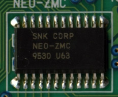
Z80 Memory Controller. Handles the Z80 bankswitching in cartridges. To save pins, the Z80's upper address line are also used as data input. The chip's write strobe SDRD0 is port address decoded inside the system.
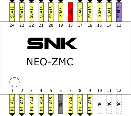
Pinout
Pins 10, 11, 12 may be M1 higher address bits ?
- SDA0, SDA1, SDA8~15: Z80 address bus
- M1 A11~M1 A18: M1 ROM address lines
- SDRD0: Decoded write signal from NEO-D0 (latch on rising edge)
Operation
SDA8~SDA15 are used for the bank number (data), SDA0 and SDA1 for selecting the window.
| SDA1 | SDA0 | Z80 port | Window | Address range | Size | Latch size |
|---|---|---|---|---|---|---|
| 0 | 0 | $08 | 0 | $F000~$F7FF | 2KiB | 8 bits |
| 0 | 1 | $09 | 1 | $E000~$EFFF | 4KiB | 7 bits |
| 1 | 0 | $0A | 2 | $C000~$DFFF | 8KiB | 6 bits |
| 1 | 1 | $0B | 3 | $8000~$BFFF | 16KiB | 5 bits |
Details

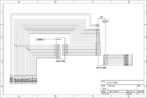
SDRD0 must be high before configuring banks.
To configure a bank to be accessed (e.g. bank 1 in the $8000~$BFFF range):
- Set SDRD0 low (prepare for new bank configuration, outputs are tri-stated)
- Set SDA0~15 = $8103, select 16KiB bank 1 in window 3 (Why $8103 and not just $0103 ?)
- Set SDRD0 high (latch bank, ready to convert inputs to proper output signals)
- Now, when the Z80 reads the $8000~BFFF range, NEO-ZMC will map this to the M1 ROM zone $04000~$07FFF
