PCM: Difference between revisions
Jump to navigation
Jump to search
mNo edit summary |
mNo edit summary |
||
| Line 6: | Line 6: | ||
On some [[cartridge board]]s, V A20~V A22 can be used to select which of the 4 possible V ROMs to use (decoded by a LS139). | On some [[cartridge board]]s, V A20~V A22 can be used to select which of the 4 possible V ROMs to use (decoded by a LS139). | ||
=Internal logic= | |||
Takes advantage of the asynchronous reading from the [[YM2610]]. See [[YM2610 bus timing]]. | |||
Verilog: todo. | |||
=Pinout= | =Pinout= | ||
Revision as of 08:39, 7 January 2013

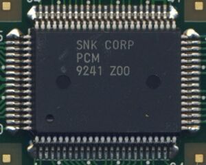
V ROM banking and multiplexing chip, found in AES and MVS cartridges, and on ROM-only arcade boards. Used to multiplex V ROM (ADPCM-A and ADPCM-B) access to mixed-content ROM chips.
NEO-PCM2 can also be found in late cartridges and with NEO-YSA2.
On some cartridge boards, V A20~V A22 can be used to select which of the 4 possible V ROMs to use (decoded by a LS139).
Internal logic
Takes advantage of the asynchronous reading from the YM2610. See YM2610 bus timing.
Verilog: todo.
Pinout
OpenOffice Draw file: File:Pcm.odg
Has an inverting gate on pins 26 and 27.
- SDPOE, SDROE, SDPMPX, SDRMPX: from the YM2610
- SDRAD0~SDRAD7: ADPCM-A multiplexed bus part
- SDPAD0~SDPAD7: ADPCM-B multiplexed bus part
- SDRA8,SDRA9,SDRA20~SDRA23: ADPCM-A address bus
- SDPA8~SDPA11: ADPCM-B address bus
- V D0~V D7: V ROM(s) data bus
- V A0~V A22: V ROM(s) address bus