NEO-273: Difference between revisions
mNo edit summary |
mNo edit summary |
||
| Line 1: | Line 1: | ||
{{ChipInfo | |||
|picture=crt_273.jpg | |||
|pkg=QFP64R | |||
|manu=fujitsu | |||
|date=1992 ? | |||
|gates= | |||
|used_on={{PCB|MVS cartridge}}s | |||
}} | |||
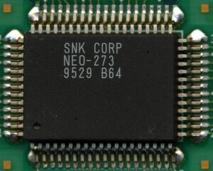
This chip is used in cartridges to replace 74LS273 and 74LS174 latches that were used in early boards (Like on [[CHA board|CHA-32]]). It demultiplexes the [[P bus]] to [[C ROM]] and [[S ROM]] addresses. | This chip is used in cartridges to replace 74LS273 and 74LS174 latches that were used in early boards (Like on [[CHA board|CHA-32]]). It demultiplexes the [[P bus]] to [[C ROM]] and [[S ROM]] addresses. | ||
Revision as of 10:03, 30 August 2016

| |
| Package | QFP64R |
| Manufacturer | |
| First use | 1992 ? |
| Used on | MVS cartridges |
This chip is used in cartridges to replace 74LS273 and 74LS174 latches that were used in early boards (Like on CHA-32). It demultiplexes the P bus to C ROM and S ROM addresses.
It includes one 16-bit latch (to address a 128KiB S ROM) and one 20-bit latch (to address 8MiB of 2*16bits C ROMs) in one package. Note that A4 (CA4) of the C ROMs and A3 (2H1) of the S ROM are not part of the multiplexed bus and come straight from the cartridge edge, bypassing this chip.
The C ROM address is latched on the rising edge of PCK1B. The S ROM address on the rising edge of PCK2B.
This chip was later replaced by NEO-CMC which performs the same function along with quite a few other things.
For cartridges that use this chip but have more than 8MiB of C ROM, extra bits were added using 7400 chips. An added LS74 (2 bits) in CHA256 boards for example increases the C ROM capacity from 8MiB to 32MiB (256M).
Demultiplexing
| external | internal | ||||||||||||||||||||||||||||
| P BUS | P23 | P22 | P21 | P20 | P19 | P18 | P17 | P16 | P15 | P14 | P13 | P12 | P11 | P10 | P9 | P8 | P7 | P6 | P5 | P4 | P3 | P2 | P1 | P0 | |||||
|---|---|---|---|---|---|---|---|---|---|---|---|---|---|---|---|---|---|---|---|---|---|---|---|---|---|---|---|---|---|
| C address | A24 | A23 | A22 | A21 | A3 | A2 | A1 | A0 | A20 | A19 | A18 | A17 | A16 | A15 | A14 | A13 | A12 | A11 | A10 | A9 | A8 | A7 | A6 | A5 | |||||
| S address | A4 | A2 | A1 | A0 | A16 | A15 | A14 | A13 | A12 | A11 | A10 | A9 | A8 | A7 | A6 | A5 | |||||||||||||
A /C_A20 signal is available on pin 47 to allow cartridges which use 2MiB C Roms to switch between 2 pairs without an additionnal inverter chip.
Pinout
OpenOffice Draw file: File:Neo-273.odg