LC8953: Difference between revisions
mNo edit summary |
mNo edit summary |
||
| Line 4: | Line 4: | ||
Both publicly available datasheets for these ICs are incomplete. | Both publicly available datasheets for these ICs are incomplete. | ||
=DMA= | |||
The datasheet describes a 16-instruction microcode that is used to control DMA registers and transfer. There is no public documentation of this (?) and all open source emulates use HLE to emulate it. 18 bytes of microcode are written by the BIOS for each type of transfer to register. The microcode can be written using 9 word writes or 4 longword writes and one word write (verified). | The datasheet describes a 16-instruction microcode that is used to control DMA registers and transfer. There is no public documentation of this (?) and all open source emulates use HLE to emulate it. 18 bytes of microcode are written by the BIOS for each type of transfer to register. The microcode can be written using 9 word writes or 4 longword writes and one word write (verified). | ||
| Line 15: | Line 15: | ||
*Set $FF0061 to $40 | *Set $FF0061 to $40 | ||
==Word fill== | |||
<pre> | <pre> | ||
| Line 25: | Line 25: | ||
</pre> | </pre> | ||
==Word copy== | |||
<pre> | <pre> | ||
| Line 36: | Line 36: | ||
</pre> | </pre> | ||
==Address fill== | |||
<pre> | <pre> | ||
| Line 45: | Line 45: | ||
</pre> | </pre> | ||
==Byte copy== | |||
<pre> | <pre> | ||
| Line 66: | Line 66: | ||
*Repeat (length) times | *Repeat (length) times | ||
= | =IRQs= | ||
There is a programmable IRQ controller in this chip but it's not known if the [[NEO-MGA]] is used for this instead. DMA is used to copy the 2KB of data into work RAM and an interrupt is generated to signal this after every sector copied (and for other events too?). This is emulated at least by MESS. | There is a programmable IRQ controller in this chip but it's not known if the [[NEO-MGA]] is used for this instead. DMA is used to copy the 2KB of data into work RAM and an interrupt is generated to signal this after every sector copied (and for other events too?). This is emulated at least by MESS. | ||
=Datasheet= | |||
Incomplete official datasheet: [[http://www.datasheetcatalog.org/datasheet/sanyo/ds_pdf_e/LC8953.pdf]] | Incomplete official datasheet: [[http://www.datasheetcatalog.org/datasheet/sanyo/ds_pdf_e/LC8953.pdf]] | ||
[[Category:Chips]] | [[Category:Chips]] | ||
[[Category:CD systems]] | |||
Revision as of 01:15, 17 November 2016

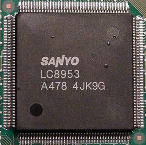
Sanyo Programmable Controler ("PUPPET") used in CD systems. Handles DMA to DRAM. Later replaced by the LC98000. Both publicly available datasheets for these ICs are incomplete.
DMA
The datasheet describes a 16-instruction microcode that is used to control DMA registers and transfer. There is no public documentation of this (?) and all open source emulates use HLE to emulate it. 18 bytes of microcode are written by the BIOS for each type of transfer to register. The microcode can be written using 9 word writes or 4 longword writes and one word write (verified).
This can be used as a reference to reverse engineer the microcode format or to control the DMA hardware without BIOS routines. These were tested working on top-loading CDM 4-x boards as part of a test routine.
- Set $FF0061 to $00
- Write microcode to $FF007E+
- Set registers as defined by microcode
- Set $FF0061 to $40
Word fill
dc.w $FFDD,$FCF5,$92F6,$2602,$FDFF,$FFFF,$FCF5,$8AF0,$1609 (CDM 4-x & CDZ)

$FF0064: 32bit destination
$FF006C: 16bit word to fill with
$FF0070: 32bit length in words
Word copy
dc.w $FE6D,$FCF5,$82BF,$F693,$BF29,$02FD,$FFFF,$F97D,$FCF5 (CDM 4-x)
dc.w $FE3D,$FCF5,$82BF,$93BF,$F629,$02FD,$FFFF,$F17D,$FCF5 (CDZ)

$FF0064: 32bit source
$FF0068: 32bit destination
$FF0070: 32bit length in words
Address fill
dc.w $FEF5,$FCF5,$92E8,$BE96,$F629,$02FD,$FFFF,$FC3D,$FCF5 (CDM 4-x & CDZ)

$FF0064: 32bit destination
$FF0070: 32bit length in longs (number of addresses to copy)
Byte copy
dc.w $F2DD,$FCF5,$82F6,$93DA,$BE93,$DABE,$2C02,$FDFF,$FFCD (CDM 4-x)
dc.w $E2DD,$FCF5,$82BE,$93DA,$BE93,$DABE,$F62D,$02FD,$FFFF (CDZ)

$FF0064: 32bit source
$FF0068: 32bit destination
$FF0070: 32bit length in words (as in pairs of bytes)
Used for copying data to 8bit memory, such as PCM RAM.
- Read word from source
- Swap word
- Write word to destination
- Swap word again
- Write word to destination + 2
- source += 2, destination += 4
- Repeat (length) times
IRQs
There is a programmable IRQ controller in this chip but it's not known if the NEO-MGA is used for this instead. DMA is used to copy the 2KB of data into work RAM and an interrupt is generated to signal this after every sector copied (and for other events too?). This is emulated at least by MESS.
Datasheet
Incomplete official datasheet: [[1]]