VRAM: Difference between revisions
m (Speed grades) |
|||
| Line 67: | Line 67: | ||
Even if VRAM can be modified at any time (even during active display), since it is not dual-ported, some timing restrictions have to be met in order to avoid skipping writes or reading data too early after setting the address. This is because the [[LSPC]] needs to interleave a number of "access slots" per video line for the CPU between rendering steps. | Even if VRAM can be modified at any time (even during active display), since it is not dual-ported, some timing restrictions have to be met in order to avoid skipping writes or reading data too early after setting the address. This is because the [[LSPC]] needs to interleave a number of "access slots" per video line for the CPU between rendering steps. | ||
== | ==Acces timing== | ||
SNK imposed minimum waiting times to always be sure that no read or write operation to VRAM will fail. This is because [[LSPC]] provides CPU access slots at a slower rate than the CPU can read or write. | SNK imposed minimum waiting times to always be sure that no read or write operation to VRAM will fail. This is because [[LSPC]] provides CPU access slots at a slower rate than the CPU can read or write. | ||
| Line 75: | Line 75: | ||
Note that these timings only affect the VRAM access, and not the other LSPC registers. | Note that these timings only affect the VRAM access, and not the other LSPC registers. | ||
==Speed== | |||
* Lower (slow) VRAM must be 120ns or less (3mclk). | |||
* Upper (fast) VRAM must be 35ns or less (1mclk). | |||
[[Category:Video system]] | [[Category:Video system]] | ||
Revision as of 09:57, 5 September 2017
VRAM stands for Video RAM.
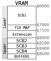
The NeoGeo has 68KiB (physically 64KiB + 4KiB, respectively called lower and upper, or slow and fast) of VRAM accessible as 16 bits words, which is used to store sprite attributes, the fix layer tile map and sprite lists for video rendering. Contrary to other systems, the VRAM here does not contain actual graphics.
Access to VRAM is done through 3 Memory mapped registers handled by the GPU, it isn't mapped in the 68k address space. Every VRAM address points to a word, not a byte.
- REG_VRAMADDR ($3C0000) sets the VRAM address for the next read/write operation
- REG_VRAMRW ($3C0002) is the data read or to write
- REG_VRAMMOD ($3C0004) is the signed value added to the VRAM address after a write
The original SNK documentation specifies that the address register should be set directly instead of using REG_VRAMMOD when crossing VRAM zones ($0000~$7FFF to/from $8000~$FFFF). This is probably because the GPU's internal adder is 15 bit only.
Memory map

| Start | End | Size | Zone | Description |
| $0000 | $6FFF | 28KiB | Lower | SCB1 |
| $7000 | $74FF | 4KiB | Fix map | |
| $7500 | $7FFF | Extension | ||
| $8000 | $81FF | 512B | Upper | SCB2 |
| $8200 | $83FF | 512B | SCB3 | |
| $8400 | $85FF | 512B | SCB4 | |
| $8600 | $867F | 128B | Sprite list for even scanlines | |
| $8680 | $86FF | 128B | Sprite list for odd scanlines |
Even if VRAM can be modified at any time (even during active display), since it is not dual-ported, some timing restrictions have to be met in order to avoid skipping writes or reading data too early after setting the address. This is because the LSPC needs to interleave a number of "access slots" per video line for the CPU between rendering steps.
Acces timing
SNK imposed minimum waiting times to always be sure that no read or write operation to VRAM will fail. This is because LSPC provides CPU access slots at a slower rate than the CPU can read or write.
- After writing the VRAM address, a read will return valid data after 16 CPU cycles or more (>32mclk).
- After writing the VRAM data, the address can set after 16 CPU cycles or more (>32mclk).
- After writing the VRAM data, another write can be done 12 CPU cycles or more (>24mclk).
Note that these timings only affect the VRAM access, and not the other LSPC registers.
Speed
- Lower (slow) VRAM must be 120ns or less (3mclk).
- Upper (fast) VRAM must be 35ns or less (1mclk).