NEO-SMA: Difference between revisions
Jump to navigation
Jump to search
m (2 revisions: Import from wikkii) |
No edit summary |
||
| Line 1: | Line 1: | ||
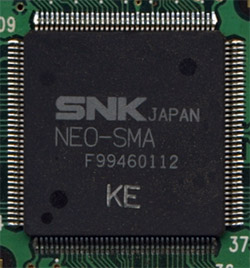
[[File:crt_sma.jpg|right|thumb|NEO-SMA chip found in a MVS cartridge. Picture courtesy of [[http://www.mvs-scans.com MVS-Scans]].]] | [[File:crt_sma.jpg|right|thumb|NEO-SMA chip found in a MVS cartridge. Picture courtesy of [[http://www.mvs-scans.com MVS-Scans]].]] | ||
QFP144 chip found connected to the [[P ROM]]s in some [[Metal Slug 3]] and [[Garou MVS MotW]] [[cartridges]]. | Info from [[http://mamedev.org/source/src/mame/machine/neoprot.c MAME's source]] | ||
QFP144 chip found connected to the [[P ROM]]s in some [[King of Fighters 99]], [[King of Fighters 2000]], [[Metal Slug 3]] and [[Garou MVS MotW]] [[cartridges]]. Bankswitches the [[68k memory map|second megabyte]] ($200000~$2FFFFF) of P ROM space and provides a 16bit pseudo random number generator. | |||
Upon system reset, the PRN is initialized to $2345. | |||
The chip always (?) replies $9A37 on reads. | |||
=PRN= | |||
16bit LSFR with taps at bits 2,3,5,6,7,11,12,15. Each read steps the register. | |||
[[File:Smalfsr.png]] | |||
=Bankswitching= | |||
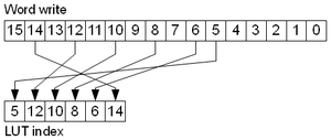
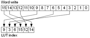
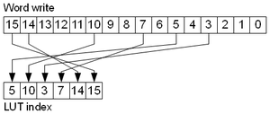
Bankswitching is done by unscrambling the written bank number and using a 64 entry (256 bytes) lookup table to map the P ROM into $200000~$2FFFFF. | |||
==KOF 99== | |||
[[File:Smabskof99.png|300px|thumb]] | |||
*Bankswitching write at $2FFFF1 | |||
*Read chip presence at $2FE447 | |||
*PRN at $2FFFF8 and $2FFFFA | |||
Bankswitch LUT (P2 ROM address): | |||
{|class="wikitable" | |||
! !!0!!1!!2!!3!!4!!5!!6!!7!!8!!9!!A!!B!!C!!D!!E!!F | |||
|- | |||
!0 | |||
|$000000||$100000||$200000||$300000||$3CC000||$4CC000||$3F2000||$4F2000||$407800||$507800||$40D000||$50D000||$417800||$517800||$420800||$520800 | |||
|- | |||
!1 | |||
|$424800||$524800||$429000||$529000||$42E800||$52E800||$431800||$531800||$54D000||$551000||$567000||$592800||$588800||$581800||$599800||$594800 | |||
|- | |||
!2 | |||
|$598000||?||?||?||?||?||?||?||?||?||?||?||?||?||?||? | |||
|} | |||
==Garou== | |||
*Bankswitching write at $2FFFC0 | |||
*Read chip presence at $2FE447 | |||
*PRN at $2FFFCC and $2FFFF0 | |||
==Metal Slug 3== | |||
[[File:Smabsms3.png|300px|thumb]] | |||
*Bankswitching write at $2FFFE5 | |||
*Read chip presence at $2FE447 | |||
*PRN at $2FFFF8 and $2FFFFA | |||
Bankswitch LUT (P2 ROM address): | |||
{|class="wikitable" | |||
! !!0!!1!!2!!3!!4!!5!!6!!7!!8!!9!!A!!B!!C!!D!!E!!F | |||
|- | |||
!0 | |||
|$000000||$020000||$040000||$060000||$070000||$090000||$0B0000||$0D0000||$0E0000||$0F0000||$120000||$130000||$140000||$150000||$180000||$190000 | |||
|- | |||
!1 | |||
|$1A0000||$1B0000||$1E0000||$1F0000||$200000||$210000||$240000||$250000||$260000||$270000||$2A0000||$2B0000||$2C0000||$2D0000||$300000||$310000 | |||
|- | |||
!2 | |||
|$320000||$330000||$360000||$370000||$380000||$390000||$3C0000||$3D0000||$400000||$410000||$440000||$450000||$460000||$470000||$4A0000||$4B0000 | |||
|- | |||
!3 | |||
|$4C0000||?||?||?||?||?||?||?||?||?||?||?||?||?||?||? | |||
|} | |||
==KOF 2000== | |||
[[File:Smabskof2k.png|300px|thumb]] | |||
*Bankswitching write at $2FFFED | |||
*Read chip presence at $2FE447 | |||
*PRN at $2FFFD8 and $2FFFDA | |||
Bankswitch LUT (P2 ROM address): | |||
{|class="wikitable" | |||
! !!0!!1!!2!!3!!4!!5!!6!!7!!8!!9!!A!!B!!C!!D!!E!!F | |||
|- | |||
!0 | |||
|$000000||$100000||$200000||$300000||$3F7800||$4F7800||$3FF800||$4FF800||$407800||$507800||$40F800||$50F800||$416800||$516800||$41D800||$51D800 | |||
|- | |||
!1 | |||
|$424000||$524000||$523800||$623800||$526000||$626000||$528000||$628000||$52A000||$62A000||$52B800||$62B800||$52D000||$62D000||$52E800||$62E800 | |||
|- | |||
!2 | |||
|$618000||$619000||$61A000||$61A800||?||?||?||?||?||?||?||?||?||?||?||? | |||
|} | |||
[[Category:Chips]] | [[Category:Chips]] | ||
Revision as of 22:54, 29 March 2012

Info from [MAME's source]
QFP144 chip found connected to the P ROMs in some King of Fighters 99, King of Fighters 2000, Metal Slug 3 and Garou MVS MotW cartridges. Bankswitches the second megabyte ($200000~$2FFFFF) of P ROM space and provides a 16bit pseudo random number generator.
Upon system reset, the PRN is initialized to $2345.
The chip always (?) replies $9A37 on reads.
PRN
16bit LSFR with taps at bits 2,3,5,6,7,11,12,15. Each read steps the register.
Bankswitching
Bankswitching is done by unscrambling the written bank number and using a 64 entry (256 bytes) lookup table to map the P ROM into $200000~$2FFFFF.
KOF 99

- Bankswitching write at $2FFFF1
- Read chip presence at $2FE447
- PRN at $2FFFF8 and $2FFFFA
Bankswitch LUT (P2 ROM address):
| 0 | 1 | 2 | 3 | 4 | 5 | 6 | 7 | 8 | 9 | A | B | C | D | E | F | |
|---|---|---|---|---|---|---|---|---|---|---|---|---|---|---|---|---|
| 0 | $000000 | $100000 | $200000 | $300000 | $3CC000 | $4CC000 | $3F2000 | $4F2000 | $407800 | $507800 | $40D000 | $50D000 | $417800 | $517800 | $420800 | $520800 |
| 1 | $424800 | $524800 | $429000 | $529000 | $42E800 | $52E800 | $431800 | $531800 | $54D000 | $551000 | $567000 | $592800 | $588800 | $581800 | $599800 | $594800 |
| 2 | $598000 | ? | ? | ? | ? | ? | ? | ? | ? | ? | ? | ? | ? | ? | ? | ? |
Garou
- Bankswitching write at $2FFFC0
- Read chip presence at $2FE447
- PRN at $2FFFCC and $2FFFF0
Metal Slug 3

- Bankswitching write at $2FFFE5
- Read chip presence at $2FE447
- PRN at $2FFFF8 and $2FFFFA
Bankswitch LUT (P2 ROM address):
| 0 | 1 | 2 | 3 | 4 | 5 | 6 | 7 | 8 | 9 | A | B | C | D | E | F | |
|---|---|---|---|---|---|---|---|---|---|---|---|---|---|---|---|---|
| 0 | $000000 | $020000 | $040000 | $060000 | $070000 | $090000 | $0B0000 | $0D0000 | $0E0000 | $0F0000 | $120000 | $130000 | $140000 | $150000 | $180000 | $190000 |
| 1 | $1A0000 | $1B0000 | $1E0000 | $1F0000 | $200000 | $210000 | $240000 | $250000 | $260000 | $270000 | $2A0000 | $2B0000 | $2C0000 | $2D0000 | $300000 | $310000 |
| 2 | $320000 | $330000 | $360000 | $370000 | $380000 | $390000 | $3C0000 | $3D0000 | $400000 | $410000 | $440000 | $450000 | $460000 | $470000 | $4A0000 | $4B0000 |
| 3 | $4C0000 | ? | ? | ? | ? | ? | ? | ? | ? | ? | ? | ? | ? | ? | ? | ? |
KOF 2000

- Bankswitching write at $2FFFED
- Read chip presence at $2FE447
- PRN at $2FFFD8 and $2FFFDA
Bankswitch LUT (P2 ROM address):
| 0 | 1 | 2 | 3 | 4 | 5 | 6 | 7 | 8 | 9 | A | B | C | D | E | F | |
|---|---|---|---|---|---|---|---|---|---|---|---|---|---|---|---|---|
| 0 | $000000 | $100000 | $200000 | $300000 | $3F7800 | $4F7800 | $3FF800 | $4FF800 | $407800 | $507800 | $40F800 | $50F800 | $416800 | $516800 | $41D800 | $51D800 |
| 1 | $424000 | $524000 | $523800 | $623800 | $526000 | $626000 | $528000 | $628000 | $52A000 | $62A000 | $52B800 | $62B800 | $52D000 | $62D000 | $52E800 | $62E800 |
| 2 | $618000 | $619000 | $61A000 | $61A800 | ? | ? | ? | ? | ? | ? | ? | ? | ? | ? | ? | ? |
