CHA board: Difference between revisions
Cyberwillis (talk | contribs) (→CHAFIO) |
Cyberwillis (talk | contribs) |
||
| Line 4: | Line 4: | ||
==CHA boards== | ==CHA boards== | ||
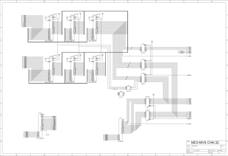
===NEO-MVS | ===NEO-MVS CHA-32=== | ||
[[File:neo-mvs-cha32.png|x600px]] | [[File:neo-mvs-cha32.png|x600px]] | ||
Revision as of 00:36, 4 December 2011
From MAME's source:
MVS
CHA boards
NEO-MVS CHA-32
CHA-8M
CHA42G
CHA42G-1
CHA 42G-2
CHA 42G-3
CHA 42G-3B
CHA256
C ROM
Up to 8x 32Mbit ROMs (27C322) can be used for a maximum of 256Mbit C ROM. 27C800/27C160 can also depending on jumper config. Size of largest ROM is selected using a pair of jumpers. The rest should be left unconnected.
| ROM size | Jumper A | Jumper B |
|---|---|---|
| 8Mbit | J5 | J6 |
| 16Mbit | J7 | J8 |
| 32Mbit | J9 | J10 |
Pinouts
A NEO-273 and a LS74 is used to address C ROM. LS74 provides the 2 most significant bits. LS139 enables one of four pairs of C ROMs using 2 address inputs depending on which 2 jumpers are connected.
| Jumper | LS139 | LS74 | NEO-273 |
|---|---|---|---|
| J5 | 2(1A) | N/A | 45(A19) |
| J6 | 3(1B) | N/A | 46(A20) |
| J7 | 2(1A) | N/A | 46(A20) |
| J8 | 3(1B) | 9(Q2) | N/A |
| J9 | 2(1A) | 9(Q2) | N/A |
| J10 | 3(1B) | 5(Q1) | N/A |
- Max 256Mbit C ROM (8x 32Mbit)
- NEO-273
- NEO-ZMC
- LS139,LS74
CHA256B
CHA512Y
- Max 8 8MiB C ROMs
- Max 128KiB M1 ROM
- Max 128KiB S1 ROM
- NEO-273
- NEO-ZMC
- LS139,LS174
CHAFIO
- used with NEO-CMC 90G06C7042 or NEO-CMC 90G06C7050
MVS CHAFIO REV1.0 (KOF-2001)
CHAFIO (SNK 2002)
CHAFIO
- Max 8x 64Mbits (4Mb x 16) C ROMs
- Max 1x 4Mbits (512Kb x8) M1 ROM
- used only with NEO-CMC 90G06CF7042 and 90G06C7050
PROG boards
PROG-NAM
PROG-HERO
PROG-EP
PROG-8MB
PROG8M42
PROG16
PROG 42G
PROG 42G-COM
PROG 42G-1
PROG-G2
PROG 4096
PROG 4096 B
PROGGSC
PROGSM
PROGSS3
PROGTOP
PROGSF1
PROGEOP
PROGLBA
PROGBK1
The only non-protected board that can bankswitch and use all V ROM space. Really common and very useful for homebrew stuff or converts.
P ROM
P1 can be 4Mbit, 8Mbit or 16Mbit (27C400/27C800/27C160).
- If P1 is 16Mbit then some jumper must be set (JB3? didn't look into it. see kof95) and P2 should be empty. First half of P1 is mapped to 0x200000-0x2FFFFF and second half is mapped to 0x000000-0x0FFFFFF.
- If P1 is 4Mbit or 8Mbit, then P2 can contain a bankswitched ROM (same type as P1 plus 27C322). P1 appears at 0x000000-0x0FFFFF. P2 banked rom appears in 0x200000-0x2FFFFF.
V ROM
V ROMs can be 8Mbit, 16Mbit or 32Mbit (27C800/27C160/27C322). Size of largest ROM is selected with a pair of jumpers and the other 4 should be left unconnected. 4Mbit can also be used but only if there is one ROM and only in the last used slot.
| ROM size | Jumper A | Jumper B |
|---|---|---|
| 8Mbit | JV1 | JV2 |
| 16Mbit | JV3 | JV4 |
| 32Mbit | JV5 | JV6 |
Pinouts
Bankswitching is done with the LS74. It's not needed if the game isn't banked. Any write to an odd 0x200000-0x2FFFFF address will set the bank.
| Cart edge | LS74 | P2 |
|---|---|---|
| A5(68k D0) | 2(D1) | N/A |
| A6(68k D1) | 12(D2) | N/A |
| A28(PORTWEL) | 3(CLK1) | N/A |
| A28(PORTWEL) | 11(CLK2) | N/A |
| N/A | 5(Q1) | 42(A19) |
| N/A | 9(Q2) | 32(A20) |
One of 4 V ROMs is enabled with a set of LS139 outputs. The pair of V ROM jumpers effectively choose a set of 2 NEO-PCM address outputs to input to the LS139.
| Jumper | LS139 | V ROM |
|---|---|---|
| JV1 | 2(1A) | N/A |
| JV2 | 3(1B) | N/A |
| JV3 | 2(1A) | N/A |
| JV4 | 3(1B) | N/A |
| JV5 | 2(1A) | N/A |
| JV6 | 3(1B) | N/A |
| N/A | 4(1Y0) | V1 13(/OE) |
| N/A | 5(1Y1) | V2 13(/OE) |
| N/A | 6(1Y2) | V3 13(/OE) |
| N/A | 7(1Y3) | V4 13(/OE) |
The LS08 is used to AND the two PORT /OE signals.
- 4x 1/2/4MiB V ROMs
- 1/2MiB P1 ROM
- 1/2/4MiB P2 ROM
- 2x 512KiB EP1/EP2 ROM
- NEO-PCM
- LS139,LS08,LS74
PROGBK2
Looks identical to PROGBK1 in terms of ROM layout but uses a NEO-PCM2 for encryption plus all other logic that was done with discrete chips on PROGBK1.
PROGBK2 REV1.0 (KOF-2001)
PROGBK2
PROGBK2R
PROGBK3R
PROGBK3S
PROGBK2S
PROGV (Brezzasoft)
Same board manufacturer as SNK ?
- 42pin V1 and P1 ROMs (DIP or TSOP)
- 64KiB Battery-backed RAM (Mapped to $200000~?)
- External I/O port (8 ?)
- Room for 2x8DIP switchs
