CHA board: Difference between revisions
Jump to navigation
Jump to search
Cyberwillis (talk | contribs) |
mNo edit summary |
||
| Line 1: | Line 1: | ||
List from [[http://mamedev.org/source/src/mame/drivers/neodrvr.c.html MAME's source]]. | |||
==CHA boards== | |||
{| class="wikitable" | |||
!Test | |||
!Test2 | |||
|- | |||
|A | |||
|B | |||
|} | |||
=MVS= | =MVS= | ||
==CHA boards== | ==CHA boards== | ||
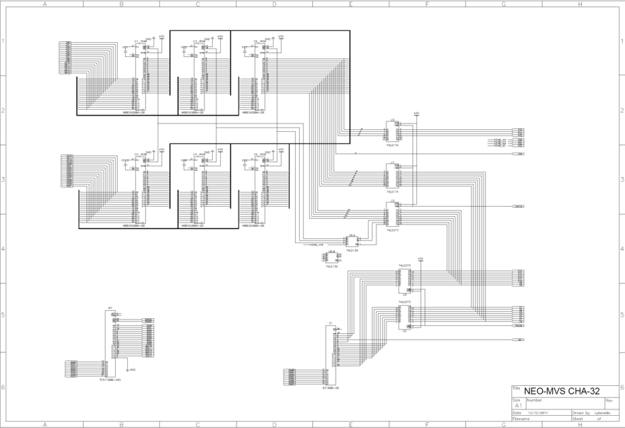
=== | ===CHA-32=== | ||
[[File:neo-mvs-cha32.png|x600px]] | [[File:neo-mvs-cha32.png|x600px]] | ||
| Line 10: | Line 19: | ||
===CHA42G=== | ===CHA42G=== | ||
===CHA42G-1=== | ===CHA42G-1=== | ||
=== | ===CHA42G-2=== | ||
=== | ===CHA42G-3=== | ||
=== | ===CHA42G-3B=== | ||
===CHA256=== | ===CHA256=== | ||
====C ROM==== | ====C ROM==== | ||
Up to 8x 32Mbit ROMs (27C322) can be used for a maximum of 256Mbit C ROM. 27C800/27C160 can also depending on jumper config. | Up to 8x 32Mbit ROMs (27C322) can be used for a maximum of 256Mbit C ROM. 27C800/27C160 can also be used depending on jumper config. Size of largest ROM is selected using a pair of jumpers. The rest should be left unconnected. | ||
{| class="wikitable" | {| class="wikitable" | ||
| Line 40: | Line 49: | ||
====Pinouts==== | ====Pinouts==== | ||
A NEO-273 and a LS74 | A [[NEO-273]] and a LS74 are used to address C ROM. LS74 provides the 2 most significant bits. LS139 enables one of four pairs of C ROMs using 2 address inputs depending on which 2 jumpers are connected. | ||
{| class="wikitable" | {| class="wikitable" | ||
| Line 81: | Line 90: | ||
*Max 256Mbit C ROM (8x 32Mbit) | *Max 256Mbit C ROM (8x 32Mbit) | ||
*NEO-273 | *[[NEO-273]] | ||
*NEO-ZMC | *[[NEO-ZMC]] | ||
*LS139,LS74 | *LS139,LS74 | ||
| Line 101: | Line 110: | ||
*Max 1x 4Mbits (512Kb x8) M1 ROM | *Max 1x 4Mbits (512Kb x8) M1 ROM | ||
*used only with NEO-CMC 90G06CF7042 and 90G06C7050 | *used only with NEO-CMC 90G06CF7042 and 90G06C7050 | ||
[[Category:Chips]] | [[Category:Chips]] | ||
[[Category:Cartridge systems]] | [[Category:Cartridge systems]] | ||
Revision as of 15:12, 13 December 2011
List from [MAME's source].
CHA boards
| Test | Test2 |
|---|---|
| A | B |
MVS
CHA boards
CHA-32
CHA-8M
CHA42G
CHA42G-1
CHA42G-2
CHA42G-3
CHA42G-3B
CHA256
C ROM
Up to 8x 32Mbit ROMs (27C322) can be used for a maximum of 256Mbit C ROM. 27C800/27C160 can also be used depending on jumper config. Size of largest ROM is selected using a pair of jumpers. The rest should be left unconnected.
| ROM size | Jumper A | Jumper B |
|---|---|---|
| 8Mbit | J5 | J6 |
| 16Mbit | J7 | J8 |
| 32Mbit | J9 | J10 |
Pinouts
A NEO-273 and a LS74 are used to address C ROM. LS74 provides the 2 most significant bits. LS139 enables one of four pairs of C ROMs using 2 address inputs depending on which 2 jumpers are connected.
| Jumper | LS139 | LS74 | NEO-273 |
|---|---|---|---|
| J5 | 2(1A) | N/A | 45(A19) |
| J6 | 3(1B) | N/A | 46(A20) |
| J7 | 2(1A) | N/A | 46(A20) |
| J8 | 3(1B) | 9(Q2) | N/A |
| J9 | 2(1A) | 9(Q2) | N/A |
| J10 | 3(1B) | 5(Q1) | N/A |
CHA256B
CHA512Y
- Max 8 8MiB C ROMs
- Max 128KiB M1 ROM
- Max 128KiB S1 ROM
- NEO-273
- NEO-ZMC
- LS139,LS174
CHAFIO
- used with NEO-CMC 90G06C7042 or NEO-CMC 90G06C7050
MVS CHAFIO REV1.0 (KOF-2001)
CHAFIO (SNK 2002)
CHAFIO
- Max 8x 64Mbits (4Mb x 16) C ROMs
- Max 1x 4Mbits (512Kb x8) M1 ROM
- used only with NEO-CMC 90G06CF7042 and 90G06C7050
