Bankswitching: Difference between revisions
(Created page with "Games which need more than 1MiB of P ROM use simple bankswitching of the "P2" ROM, which is achieved in hardware by D-latches on the PROG board. The P1 ROM is always (?) ...") |
(No difference)
|
Revision as of 00:52, 11 February 2012
Games which need more than 1MiB of P ROM use simple bankswitching of the "P2" ROM, which is achieved in hardware by D-latches on the PROG board. The P1 ROM is always (?) fixed (in $000000~$1FFFFF ?).
To switch the ROM data in the $200000~$2FFFFF range, a byte needs to be written in this range. Depending on how many D-latches are connected to the 68k data bus, one or more bits can be used to switch banks.

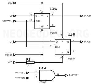
For example, the PROGBK1 board uses a 74LS74 dual D-latch to allow a 4MiB P2 ROM to be mapped with 4, 1MiB banks (see schematic).
In this case, when a byte write is made in the $200000~$2FFFFF range, PORTWEL drops, latching D0 and D1 to the P2's A20 and A21 lines respectively. When the NeoGeo is reset, both latches are set to 0, to ensure that the first bank is mapped on startup.
(Why is there a pullup on RESET ?)
As there is no /PORTOE signal on the cartridge edge (like /ROMOE), both /PORTOEL and /PORTOEU needs to be ANDed together to make the /OE signal of P2 (if it's a 16bit ROM).
Example code
move.b #3,#$200000    ;Puts P2's $300000~$3FFFFF in $200000~$2FFFFF
move.b #1,#$2B92F1    ;Puts P2's $100000~$1FFFFF in $200000~$2FFFFF