NEO-ZMC2: Difference between revisions
Jump to navigation
Jump to search
mNo edit summary |
mNo edit summary |
||
| Line 1: | Line 1: | ||
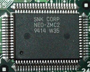
[[File:mvs_zmc2.jpg|right|thumb|NEO-ZMC2 chip found on a 1FZS MVS board.]] | [[File:mvs_zmc2.jpg|right|thumb|NEO-ZMC2 chip found on a 1FZS MVS board.]] | ||
[[NEO-ZMC]] and [[PRO-CT0]] in one package. The PRO-CT0 is a network of | [[NEO-ZMC]] and [[PRO-CT0]] in one package. The PRO-CT0 is a network of multiplexers (32-bit [[C ROM]] bus to two [[sprite graphics format|4 bpp]] pixel outputs). | ||
Found in second revision MVS boards (for the PRO-CT0 logic only) and AES carts. | Found in second revision MVS boards (for the PRO-CT0 logic only) and AES carts. | ||
| Line 16: | Line 16: | ||
"SORD0" = SDRD0 | "SORD0" = SDRD0 | ||
PRO-CT0 part: | PRO-CT0 part, inputs: | ||
*12M: | *12M: 12MHz clock, outputs next pixel on falling edge. | ||
*C0~C31: C ROM data bus (2*16 bits). Gives all the pixel data needed for a 8 pixel line. | |||
*LOAD: Latch C ROM data (on rising edge ?). | |||
*EVEN: Swap A/B pixels. | |||
*C0~C31: | Outpus: | ||
*DOTA: High when pixel A is opaque (color > 0) | |||
*DOTB: High when pixel B is opaque (color > 0) | |||
*GAD0~GAD3: Pixel A color data | |||
*GBD0~GBD3: Pixel B color data | |||
*H: Input, when high, reverse bit order of pixels (used for [[sprites]] horizontal flipping) | *H: Input, when high, reverse bit order of pixels (used for [[sprites]] horizontal flipping) | ||
[[Category:Chips]] | [[Category:Chips]] | ||
Revision as of 23:57, 27 June 2012

NEO-ZMC and PRO-CT0 in one package. The PRO-CT0 is a network of multiplexers (32-bit C ROM bus to two 4 bpp pixel outputs).
Found in second revision MVS boards (for the PRO-CT0 logic only) and AES carts.
Pinout
OpenOffice Draw file: File:Neo-zmc2.odg
NEO-ZMC part:
- A0,A1,A8~A15: Z80 address bus
- MA11~M21: M ROM address outputs (NEO-ZMC part)
"SORD0" = SDRD0
PRO-CT0 part, inputs:
- 12M: 12MHz clock, outputs next pixel on falling edge.
- C0~C31: C ROM data bus (2*16 bits). Gives all the pixel data needed for a 8 pixel line.
- LOAD: Latch C ROM data (on rising edge ?).
- EVEN: Swap A/B pixels.
Outpus:
- DOTA: High when pixel A is opaque (color > 0)
- DOTB: High when pixel B is opaque (color > 0)
- GAD0~GAD3: Pixel A color data
- GBD0~GBD3: Pixel B color data
- H: Input, when high, reverse bit order of pixels (used for sprites horizontal flipping)