Memory card: Difference between revisions
Jump to navigation
Jump to search
mNo edit summary |
mNo edit summary |
||
| Line 3: | Line 3: | ||
[[File:snkmemcard.jpg|thumb|Picture by [[User:HPMAN|HPMAN]]]] | [[File:snkmemcard.jpg|thumb|Picture by [[User:HPMAN|HPMAN]]]] | ||
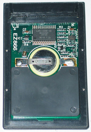
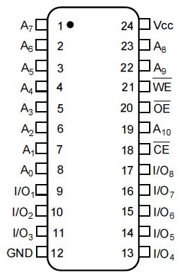
The official SNK memory card was a battery-based 2KiB card using a LH5116 CMOS SRAM chip and voltage switching circuitry. | The official SNK memory card was a battery-based 2KiB card using a LH5116 CMOS SRAM chip and voltage switching circuitry. Data retention voltage: 2V. | ||
The SP-S2 [[BIOS]] can only handle 8bit memory cards up to 16KiB ? (bank checking while format up to $8000/2). | The SP-S2 [[BIOS]] can only handle 8bit memory cards up to 16KiB ? (bank checking while format up to $8000/2). | ||
Revision as of 10:02, 6 July 2012
JEIDA V3 memory cards used in AES and some MVS systems to store game saves and/or high scores. The original SNK card could only hold 2KiB of data. The Neogeo can use up to 8MiB (24 address lines but A23 never used) ?

The official SNK memory card was a battery-based 2KiB card using a LH5116 CMOS SRAM chip and voltage switching circuitry. Data retention voltage: 2V.
The SP-S2 BIOS can only handle 8bit memory cards up to 16KiB ? (bank checking while format up to $8000/2). Seems the file checking can only go up to 256 so 16 files * 16 games * 64 bytes = 16KiB too.
Replaced by a 8KiB fixed battery-backed RAM chip in the CD systems.
See the CARD BIOS call description for memory card operations.
[Data format (from Raregame.ru)]
Data format
To do.
Card pinout

| Pin | Goes to | Signal name | PC Card name |
| 1 | GND | ||
| 2 | 9 G0 | MCD3 | D3 |
| 3 | 11 G0 | MCD4 | D4 |
| 4 | 12 G0 | MCD5 | D5 |
| 5 | 13 G0 | MCD6 | D6 |
| 6 | 14 G0 | MCD7 | D7 |
| 7 | 42, 27 C1 | CRDC | /CE1 |
| 8 | 23 E0 | Y10 | A10 |
| 9 | 30 C1 | CRDO | /OE |
| 10 | 24 E0 | Y11 | A11 |
| 11 | 22 E0 | Y9 | A9 |
| 12 | 14 E0 | Y8 | A8 |
| 13 | 28 E0 | Y13 | A13 |
| 14 | 29 E0 | Y14 | A14 |
| 15 | 6 HC32 | (31 C1 (CRDW) OR REG_CRDUNLOCK1 OR /REG_CRDUNLOCK2) | WE# |
| 16 | NC | READY | |
| 17 | VCC | ||
| 18 | VCC | ||
| 19 | 39 E0 | Y16 | A16 |
| 20 | 30 E0 | Y15 | A15 |
| 21 | 27 E0 | Y12 | A12 |
| 22 | 13 E0 | Y7 | A7 |
| 23 | 12 E0 | Y6 | A6 |
| 24 | 11 E0 | Y5 | A5 |
| 25 | 9 E0 | Y4 | A4 |
| 26 | 8 E0 | Y3 | A3 |
| 27 | 7 E0 | Y2 | A2 |
| 28 | 6 E0 | Y1 | A1 |
| 29 | 5 E0 | Y0 | A0 |
| 30 | 6 G0 | MCD0 | D0 |
| 31 | 7 G0 | MCD1 | D1 |
| 32 | 8 G0 | MCD2 | D2 |
| 33 | 88 C1 | IN26 (REG_STATUS_B bit 6) | WP |
| 34 | GND | ||
| Pin | Goes to | Signal name | PC Card name |
| 35 | GND | ||
| 36 | 73 C1 | IN24 (REG_STATUS_B bit 4) | /CD1 |
| 37 | 30 G0 | MCD11 | D11 |
| 38 | 43 G0 | MCD12 | D12 |
| 39 | 44 G0 | MCD13 | D13 |
| 40 | 45 G0 | MCD14 | D14 |
| 41 | 46 G0 | MCD15 | D15 |
| 42 | 7 | /CE2 | |
| 43 | NC | VS1# | |
| 44 | NC | IORD# | |
| 45 | NC | IOWR# | |
| 46 | 40 E0 | Y17 | A17 |
| 47 | 41 E0 | Y18 | A18 |
| 48 | 43 E0 | Y19 | A19 |
| 49 | 44 E0 | Y20 | A20 |
| 50 | 45 E0 | Y21 | A21 |
| 51 | VCC | ||
| 52 | VCC | ||
| 53 | 46 E0 | Y22 | A22 |
| 54 | 47 E0 | Y23 | A23 |
| 55 | NC | A24 | |
| 56 | NC | A25 | |
| 57 | NC | /VS2 | |
| 58 | NC | RESET | |
| 59 | NC | /WAIT | |
| 60 | NC | Reserved | |
| 61 | 8 HC32 | (REG_CRDREGSEL OR CRDO) | /REG |
| 62 | NC | BVD2 | |
| 63 | NC | BVD1 | |
| 64 | 27 G0 | MCD8 | D8 |
| 65 | 28 G0 | MCD9 | D9 |
| 66 | 29 G0 | MCD10 | D10 |
| 67 | 87 C1 | IN25 (REG_STATUS_B bit 5) | /CD2 |
| 68 | GND | ||