Video PLL: Difference between revisions
(Created page with "The video PLL circuit is only present in home consoles, it was added as a way to improve '''composite''' video quality by adjusting the main clock frequency with the color bur...") |
(No difference)
|
Revision as of 05:32, 27 August 2016
The video PLL circuit is only present in home consoles, it was added as a way to improve composite video quality by adjusting the main clock frequency with the color burst frequency.
Operation

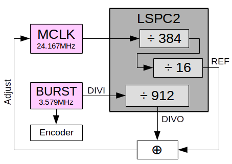
REF is generated by LSPC2-A2from the 24M main clock: Square, 24167829Hz / 384 / 16 = 3933Hz (16 lines)
DIVO is generated by LSPC2 from DIVI (color burst frequency, NTSC 3579545Hz): Not square, DIVO is counter's 10th bit (512 DIVI periods low) and reset at 912 (398 DIVI periods high ?) = 3933Hz also.
DIVO and REF are compared to generate to adjustment voltage for the varicap diode to make sure 24M = DIVI / 910 * 16 * 384 ?
DIVI also feeds the video encoder.
First generation

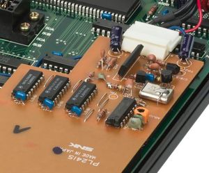
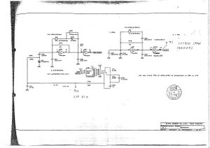
It was added during the production of first generation AES consoles as a correction board wired to different locations on the main board.
The divider was made using 74LS161 4-bit counters.
Board's reference is PL241S ?
Second generation

When SNK made the second generation chipset, the bodge became part of the system with the inclusion of the divider logic in LSPC2-A2.