MV1A: Difference between revisions
Jump to navigation
Jump to search
m (Link to PAL page) |
m (NEO-BUF roles) |
||
| Line 23: | Line 23: | ||
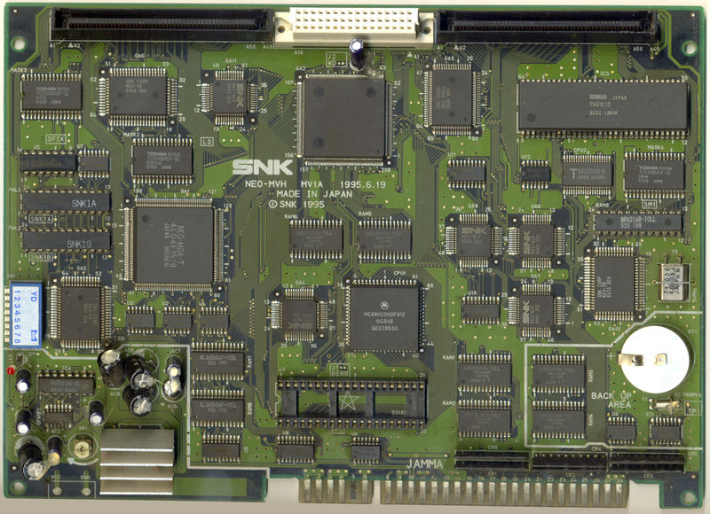
[[File:NEO-MVH MV1A Front.jpg|800px|thumb|center|Main Board Front]] | [[File:NEO-MVH MV1A Front.jpg|800px|thumb|center|Main Board Front]] | ||
{{Chipname|NEO-BUF}} list: | |||
*GA4: 68k bidirectional palette access | |||
*GA7: Read P1 and P2 inputs | |||
*GA8: Only half used, read REG_STATUS_B | |||
*GA9: 68k/Z80 communication | |||
*GA11: 68k data bus bidirectional buffer | |||
Others: | |||
*U10: 68k to Z80 latch | |||
*U11: Z80 to 68k latch | |||
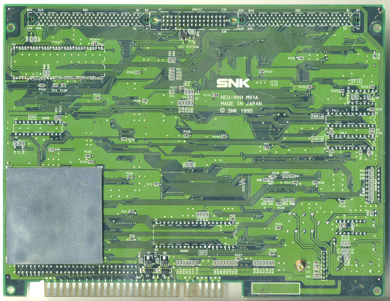
[[File:NEO-MVH MV1A Back.jpg|800px|thumb|center|Main Board Back]] | [[File:NEO-MVH MV1A Back.jpg|800px|thumb|center|Main Board Back]] | ||
Revision as of 07:23, 11 May 2018
Description
A strangely designed MVS board which uses some chips found in the NeoGeo CD. Maybe allowed SNK to cut costs by using chips for both systems.
| Specification | |
| Year | Circa 1995 |
| Number of slots | 1 |
| System ROM | Socketed |
| Cart orientation | horizontal |
| Memory Card support | no |
| Joystick support | no |
| Stereo output | no |
| Headphone output | no |
PALs
See MV1A PALs.
Scans
Main Board

NEO-BUF list:
- GA4: 68k bidirectional palette access
- GA7: Read P1 and P2 inputs
- GA8: Only half used, read REG_STATUS_B
- GA9: 68k/Z80 communication
- GA11: 68k data bus bidirectional buffer
Others:
- U10: 68k to Z80 latch
- U11: Z80 to 68k latch

Slot Board

