NEO-BUF: Difference between revisions
Jump to navigation
Jump to search
mNo edit summary |
No edit summary |
||
| Line 13: | Line 13: | ||
Also found on late [[MVS hardware|MVS]] boards. | Also found on late [[MVS hardware|MVS]] boards. | ||
== Pinout == | ==Pinout== | ||
[[File:Neo-buf_pinout.png]] | [[File:Neo-buf_pinout.png]] | ||
OpenOffice Draw file: [[File:neo-buf.odg]] | OpenOffice Draw file: [[File:neo-buf.odg]] | ||
==Replacement== | |||
[[File:Neo-buf_bypass.jpg|thumb|Picture from MVS-Scans]] | |||
On some MVS boards, some NEO-BUF chips are just used as buffers for the [[68k]] data bus. There are reports of succesful repairs done by replacing them with a small bypass board which simply connects the A side with the B side (see picture). | |||
Note that this should '''NOT''' be done to replace damaged NEO-BUF chips which are used for other purposes. This can only work for: | |||
* GA1 on the SLOT1B board of the {{PCB|MV1B}} | |||
* GA11 on the {{PCB|MV1A}} | |||
[[Category:Chips]] | [[Category:Chips]] | ||
[[Category:Repairs]] | |||
Revision as of 12:45, 8 June 2018

| |
| Package | QFP48 |
| Manufacturer | |
| First use | 1994 ? |
| Used on | MV1A MV1B NEO-CDM3-2_board |
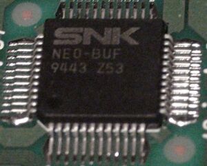
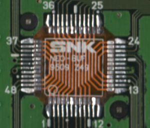
Dual 74HC245 octal transceivers in one chip. This chip is extensively used in CD systems to multiplex subsystem and 68k accesses to DRAMs.
Also found on late MVS boards.
Pinout
OpenOffice Draw file: File:Neo-buf.odg
Replacement

On some MVS boards, some NEO-BUF chips are just used as buffers for the 68k data bus. There are reports of succesful repairs done by replacing them with a small bypass board which simply connects the A side with the B side (see picture).
Note that this should NOT be done to replace damaged NEO-BUF chips which are used for other purposes. This can only work for: