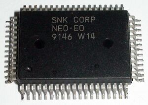
NEO-E0

Also found on MVS boards, even those without memory card slots.
BIOS vector table swapping
When 68k A8~A23 = 0 and the BIOS's vector table is chosen (by using REG_SWPBIOS or REG_SWPROM), A22I~A23I outputs are set to 1. This makes the address appear to address decoding chips as a BIOS access instead of a P ROM access.
Memory card address latch
On AES systems, BNK0~BNK2 are tied low. This makes the chip act just like a buffer ? What are BNK0~BNK2 used for ?
The chip also ANDs the pair of 8bit output enable signals from the NEO-C1 since there is only a single 16bit ROM used for the BIOS.
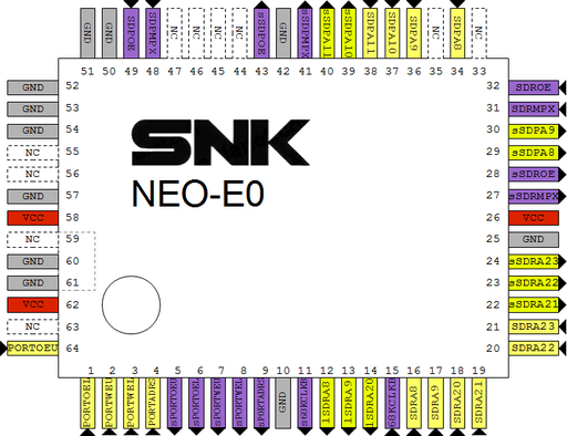
MV2B @ G2 pinout
|
OpenOffice Draw file: File:Neo-e0 mv2b G2.odg |
|
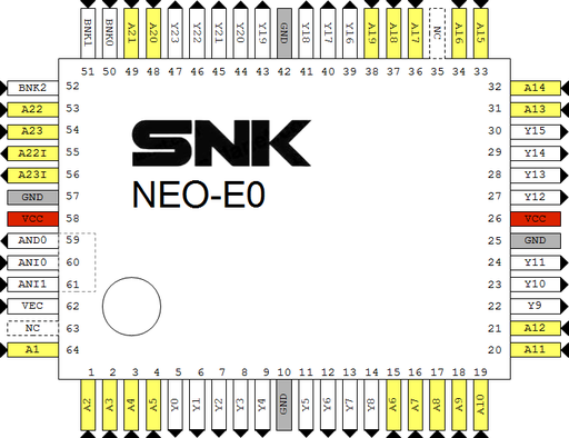
MV2B @ F7 pinout
|
OpenOffice Draw file: File:Neo-e0 mv2b F7.odg |
Acts just as a buffer.
|
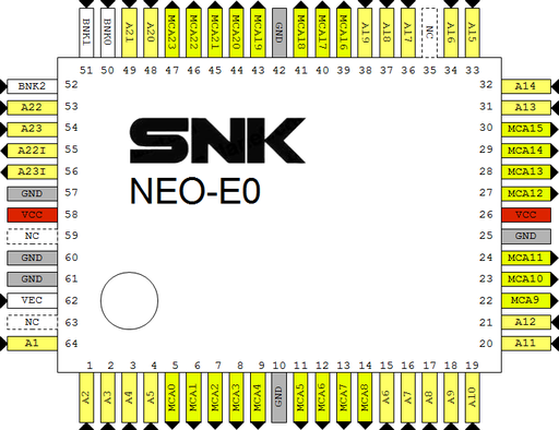
Pinout
|
OpenOffice Draw file: File:Neo-e0.odg |
|


