PROG board
Cartridge PCB which holds the P (68k code) and V (sound) ROMs.
List from [MAME's source].
MVS
| Name | Test | Max P ROM | Max V ROM |
|---|---|---|---|
| NPS-PRG1 | [[UPD4990], BR4090, PCM | ||
| PROG-8MB | |||
| PROG-EP | |||
| PROG-G2 | PCM,SNK-9201 | 512*2(+/?)1024 | |
| PROG-HERO | |||
| PROG-NAM | |||
| PROG16 | |||
| PROG4096 | PCM | 2*512+1024+2048 | 3*2048 |
| PROG4096B | |||
| PROG42G | |||
| PROG42G-1 | PCM | 128+1024 | 4*1024 |
| PROG42G-COM | |||
| PROG8M42 | |||
| PROGBK1 | |||
| PROGBK2 | |||
| PROGBK2R | |||
| PROGBK2S | |||
| PROGBK3R | |||
| PROGBK3S | |||
| PROGEOP | |||
| PROGGSC | |||
| PROGLBA | |||
| PROGTOP | |||
| PROGV | |||
| PROGMC2 | PCM | 8192 | 8192 |
NPS-PRG1
Neo Print cartridge. Has an UPD4990 and a BR4090 serial EEPROM.
PROG-8MB
PROG-EP
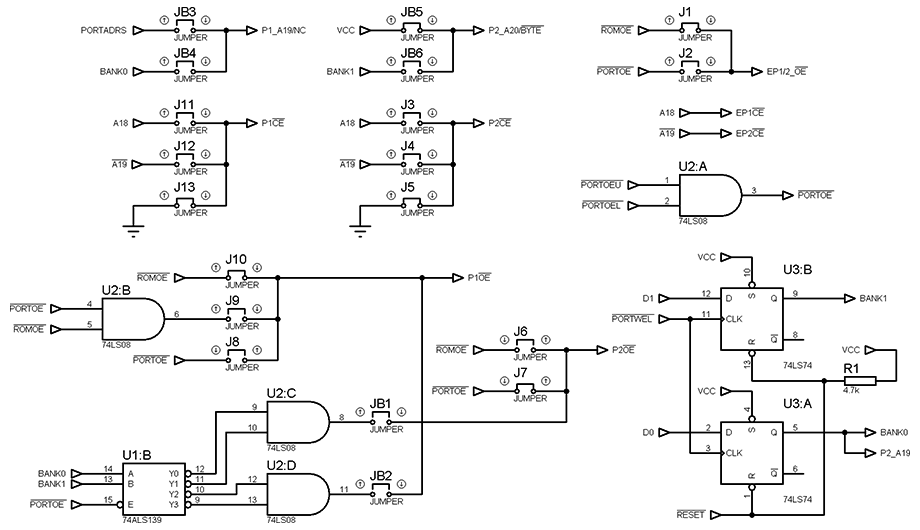
J1/J2: ROMWAIT (B25) on cart edge.
PROG-G2
PROG-HERO
PROG-NAM
PROG16
PROG4096
PROG4096B
PROG42G
PROG42G-1
PROG42G-COM
PROG8M42
PROGBK1
The only non-protected board that can bankswitch and use all V ROM space. Really common and very useful for homebrew stuff or converts.
P ROMs
| J1 | J2 |
|---|---|
| EP ROMs /OE are /ROMOE | EP ROMs /OE are /PORTOE |
| J3 | J4 | J5 |
|---|---|---|
| P2 /CE is A18 | P2 /CE is /A19 | P2 /CE is GND (default) |
| J6 | J7 | JB1 |
|---|---|---|
| P2 /OE is /ROMOE | P2 /OE is /PORTOE (default) | P2 /OE is /PORTOE, banks 0 and 1 |
| J8 | J9 | J10 | JB2 |
|---|---|---|---|
| P1 /OE is /PORTOE | P1 /OE is /PORTOE AND /ROMOE | P1 /OE is /ROMOE (default) | P1 /OE is /PORTOE, banks 2 and 3 |
| J11 | J12 | J13 |
|---|---|---|
| P1 /CE is A18 | P1 /CE is /A19 | P1 /CE is GND (default) |
| JB3 | JB4 | Nothing |
|---|---|---|
| P1 A19/NC is /PORTADRS | P1 A19/NC is BANK0 (P1 is 16Mbit) | P1 is 8Mbit |
| JB5 | JB6 |
|---|---|
| P2 A20//BYTE is VCC (P2 is 16Mbit or less) | P2 A20//BYTE is BANK1 (P2 is 32Mbit) |
The P1 ROM can be 4Mbit, 8Mbit or 16Mbit (27C400/27C800/27C160).
- ROMs can be halved and mapped to 0x000000~0x0FFFFF or 0x200000~0x2FFFFF.
- If P1 is 4Mbit or 8Mbit, then P2 can contain a bankswitched ROM (same type as P1 plus 27C322). P1 appears in 0x000000~0x0FFFFF. P2 bank appears in 0x200000~0x2FFFFF.
Bankswitching is done with the LS74. It's not needed if the game isn't banked. Any write to an odd address in the 0x200000~0x2FFFFF range will set the bank.
V ROM
There is a maximum of 4 V ROMs which can be 8Mbit, 16Mbit or 32Mbit (27C800/27C160/27C322) for a maximum total size of 4 * 4MiB = 16MiB.
A 4Mbit ROM can also be used, but only if there's one and only if it's in the last used slot.
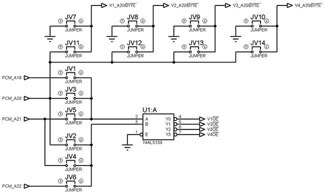
The size of the largest V ROM is selected with a pair of jumpers on 6 spots (3 possible choices).
| Largest V ROM | Jumper set |
|---|---|
| 8Mbit (1MiB) | JV1+JV2 |
| 16Mbit (2MiB) | JV3+JV4 |
| 32Mbit (4MiB) | JV5+JV6 |
This pair of V ROM jumpers effectively choose a set of 2 of the PCM chip address outputs to input to the LS139, which will enable one out of the 4 V ROMs at a time.
The JV7 to JV14 jumpers need to be set according to the ROM types. If it's less than 32Mbit, the JV7/JV8/JV9/JV10 jumper needs to be set (ground). If it's 32Mbit, the JV11/JV12/JV13/JV14 needs to be set (A20). This is because 32Mbit chips have their /BYTE pin replaced by A20.
Other
The LS08 is used to AND the /PORTOEU and /PORTOEL signals to get a /PORTOE.
- 4x 1/2/4MiB V ROMs
- 1/2MiB P1 ROM
- 1/2/4MiB P2 ROM
- 2x 512KiB EP1/EP2 ROM
- PCM chip
- LS139,LS08,LS74
PROGBK2
Looks identical to PROGBK1 in terms of ROM layout but uses a NEO-PCM2 for encryption plus all other logic that was done with discrete chips on PROGBK1.
PROGBK2R
PROGBK2S
PROGBK3R
PROGBK3S
PROGEOP
PROGGSC
PROGLBA
PROGSM
PROGSS3
PROGSF1
PROGTOP
PROGV (Brezzasoft)
Same board manufacturer as SNK ?
- 42pin V1 and P1 ROMs (DIP or TSOP)
- 64KiB Battery-backed RAM (Mapped to $200000~?)
- External I/O port (8 ?)
- Room for 2x8DIP switchs

