VRAM
VRAM stands for Video RAM.
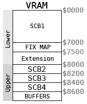
The NeoGeo has 68KiB of VRAM split in two: a 64KiB lower zone, and 4KiB higher zone. Contrary to other systems, the VRAM does not contain actual graphics. It is used to store sprite attributes, the fix layer tile map and sprite lists for video rendering.
Access to VRAM is always done through 3 memory mapped registers handled by the LSPC, it does not appear in the 68k address space. Every VRAM address points to a 16-bit word, not a byte.
- REG_VRAMADDR ($3C0000) sets the VRAM address for the next read/write operation.
- REG_VRAMRW ($3C0002) is the data read or to write.
- REG_VRAMMOD ($3C0004) is the signed value automatically added to the VRAM address after a write.
Due to the different access slots used internally for each of the VRAM zones, the address register muts be set directly instead of relying on REG_VRAMMOD to cross zones ($0000~$7FFF to/from $8000~$FFFF).
Memory map

| Start | End | Words | Zone | Description |
| $0000 | $6FFF | 28K | Lower | SCB1 |
| $7000 | $74FF | 4K | Fix map | |
| $7500 | $7FFF | Extension | ||
| $8000 | $81FF | 512 | Upper | SCB2 |
| $8200 | $83FF | 512 | SCB3 | |
| $8400 | $85FF | 512 | SCB4 | |
| $8600 | $867F | 128 | Sprite list for even scanlines | |
| $8680 | $86FF | 128 | Sprite list for odd scanlines | |
| $8700 | $87FF | 256 | Unused (free) |
Acces timing
Even if VRAM can be modified even during active display, some timing restrictions have to be met in order to avoid skipping writes or reading incorrect data. This is because the LSPC can only provide a limited number of access slots for the CPU between the video rendering steps.
SNK imposed minimum waiting times to always be sure that no read or write operation to VRAM will fail:
- After writing the VRAM address, a read will return valid data after 16 CPU cycles or more (>32mclk).
- After writing the VRAM data, a new address can be set after 16 CPU cycles or more (>32mclk).
- After writing the VRAM data, another write can be done after 12 CPU cycles or more (>24mclk).
Note that these restrictions only concern the VRAM access, and not the other LSPC registers.
Overclocked systems often produce video glitches because games are trying to access VRAM too quickly.
Speed
- Lower (slow) VRAM must be 120ns or less (3mclk).
- Upper (fast) VRAM must be 35ns or less (1mclk).