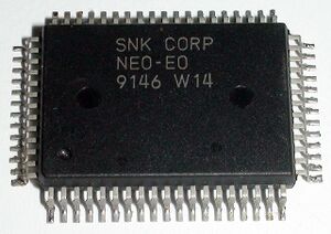
NEO-E0

| |
| Package | QFP64R |
| Manufacturer | |
| First use | 1991 ? |
| Used on | NEO-AES3-3 ... |
Just a 24-bit buffer and logic for 68k vector table swapping.
68k vector table swapping
The 68k vector table is selected between the one from the game, or the on from the system ROM by writing to REG_SWPROM or REG_SWPBIOS.
A22Z and A23Z are used in place of A22 and A23 to make the address appear to address decoding chips as a system ROM access instead of a P ROM access.
The VEC signal comes from the 74H259 system latch.
| Address | Maps to | |
|---|---|---|
| VEC = 0 | VEC = 1 | |
| $000000~$00007F | $C00000~$C0007F | $000000~$00007F |
| $000080~$BFFFFF | $000080~$BFFFFF | |
| $C00000~$C0007F | $000000~$00007F | $C00000~$C0007F |
| $C00080~$FFFFFF | $C00080~$FFFFFF | |
Verilog from User:Kyuusaku:
{A23Z,A22Z} = A[23:22] ^ 2{~|{A[21:7],^A[23:22],VEC}}
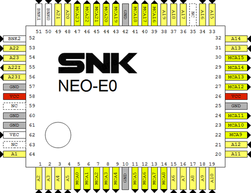
Pinouts
Input to output map
- 64 -> 5
- 1 -> 6
- 2 -> 7
- 3 -> 8
- 4 -> 9
- 15 -> 11
- 16 -> 12
- 17 -> 13
- 18 -> 14
- 19 -> 22
- 20 -> 23
- 21 -> 24
- 31 -> 27
- 32 -> 28
- 33 -> 29
- 34 -> 30
- 36 -> 39
- 37 -> 40
- 38 -> 41
- 48 -> 43
- 49 -> 44
- 50 -> 45
- 51 -> 46
- 52 -> 47
- 53 -> 55 if VEC is high
- 54 -> 56 if VEC is high
Console
On the AES, the AND gate is used to make /SROMOE from (/SROMOEL AND /SROMOEU).
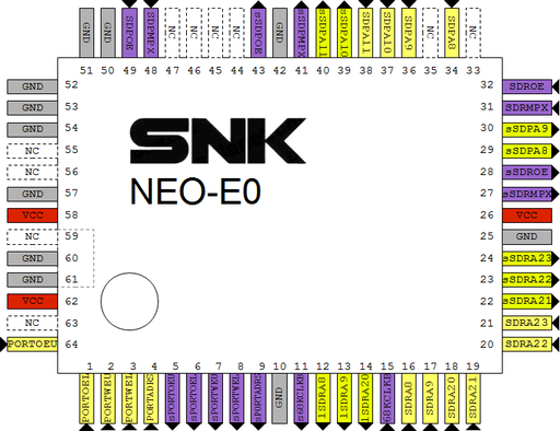
MV2B & MV2-01 @ H7 pinout
- 55 = sPCK1B
- 56 = sPCK2B
P_bus buffer
MV2B @ G2 pinout
|
OpenOffice Draw file: File:Neo-e0 mv2b G2.odg |
|
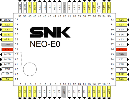
MV2B @ F7 pinout
|
OpenOffice Draw file: File:Neo-e0 mv2b F7.odg |
Acts just as a buffer.
|
MV2F @ E1 pinout (to be confirmed)
|
OpenOffice Draw file: File:Neo-e0.odg |
|


