Memory card
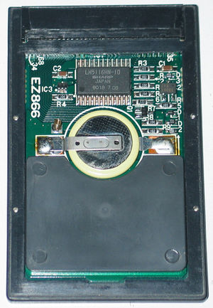
JEIDA V3 memory cards used in AES and some MVS systems to store game saves and/or high scores. The original SNK card could only hold 2KiB of data. The Neogeo can use up to 8MiB (24 address lines but A23 never used) ?

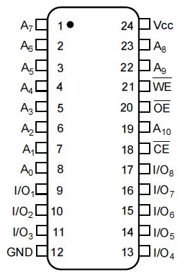
The official SNK memory card was a battery-based 2KiB card using a LH5116 CMOS SRAM chip and voltage switching circuitry. Data retention voltage: 2V.
The SP-S2 BIOS can only handle 8bit memory cards up to 16KiB ? (bank checking while format up to $8000/2). Seems the file checking can only go up to 256 so 16 files * 16 games * 64 bytes = 16KiB too.
Replaced by a 8KiB fixed battery-backed RAM chip in the CD systems.
See the CARD BIOS call description for memory card operations.
Data format
BIOS can handle 8 different card size (2K, 4K, 6K, 8K, 10K, 14K and 16K) and different card type (8 bits wide, 16 bits wide, 16 bits doubled wide and SNK ROM card).
All the data here are for all the card, it's just a matter on how to read the data between different type of card.
The internal card data are splitted into 5 regions.
Header
Always $80 bytes.
| Address | Name | Size | Description |
| $0~$9 | 10 bytes | Zero or "SNK ROM " (Development unit I think)
For 16bits doubled card, $6 is set to $0001 | |
| $A | CARD_SIZE | word | Size of the memcard |
| $C | byte | 0 | |
| $D | CARD_FAT_1_CHKSUM | byte | Checksum of the FAT 1 |
| $E | CARD_FAT_2_CHKSUM | byte | Checksum of the FAT 2 |
| $F | CARD_USERNAME_AVAILABLE | byte | 0 : Username available, !0 : Username unavailable |
| $10 | CARD_USERNAME | 16 bytes | Card holder username |
| $20 | CARD_MAGIC | 16 bytes | $4e $XX $45 $XX $4f $XX $2d $XX $47 $XX $45 $XX $4f $XX 80 $XX "NEO-GEO" + $80 |
| $30 | CARD_REGION | byte | Region of slot that formated the card, 0 = Japan, 1 = USA, 2 = Europe |
Directory
List of saves. Size depends on card size, it can hold 32, 64, 96, 128, 160, 192, 224 or 256 entries.
Each entry have this format :
| Address | Size | Description |
| $0 | byte | Game Sub number (CARD_SUB), 0 to 15. $FF if entry is free |
| $1 | word | Game NGH number |
| $3 | byte | FAT entry number (see below) |
FAT 1
List of used blocks. Size depends on card size, it can hold 64, 128 192 or 256 entries. $02 is a BIOS reserved block $01 is a game used block $00 is a free block
FAT 2
FAT 2 is simply a mirror of FAT 1.
Game Data
Normally 64 bytes but maybe some games use more that one block ?
The first 20 bytes are the data title (generally the game name + the stage name).
Card pinout

| Pin | Goes to | Signal name | PC Card name |
| 1 | GND | ||
| 2 | 9 G0 | MCD3 | D3 |
| 3 | 11 G0 | MCD4 | D4 |
| 4 | 12 G0 | MCD5 | D5 |
| 5 | 13 G0 | MCD6 | D6 |
| 6 | 14 G0 | MCD7 | D7 |
| 7 | 42, 27 C1 | CRDC | /CE1 |
| 8 | 23 E0 | Y10 | A10 |
| 9 | 30 C1 | CRDO | /OE |
| 10 | 24 E0 | Y11 | A11 |
| 11 | 22 E0 | Y9 | A9 |
| 12 | 14 E0 | Y8 | A8 |
| 13 | 28 E0 | Y13 | A13 |
| 14 | 29 E0 | Y14 | A14 |
| 15 | 6 HC32 | (31 C1 (CRDW) OR REG_CRDUNLOCK1 OR /REG_CRDUNLOCK2) | /WE |
| 16 | NC | READY | |
| 17 | VCC | ||
| 18 | VCC | ||
| 19 | 39 E0 | Y16 | A16 |
| 20 | 30 E0 | Y15 | A15 |
| 21 | 27 E0 | Y12 | A12 |
| 22 | 13 E0 | Y7 | A7 |
| 23 | 12 E0 | Y6 | A6 |
| 24 | 11 E0 | Y5 | A5 |
| 25 | 9 E0 | Y4 | A4 |
| 26 | 8 E0 | Y3 | A3 |
| 27 | 7 E0 | Y2 | A2 |
| 28 | 6 E0 | Y1 | A1 |
| 29 | 5 E0 | Y0 | A0 |
| 30 | 6 G0 | MCD0 | D0 |
| 31 | 7 G0 | MCD1 | D1 |
| 32 | 8 G0 | MCD2 | D2 |
| 33 | 88 C1 | IN26 (REG_STATUS_B bit 6) | WP (Write Protect) |
| 34 | GND | ||
| Pin | Goes to | Signal name | PC Card name |
| 35 | GND | ||
| 36 | 73 C1 | IN24 (REG_STATUS_B bit 4) | /CD1 (Card Detect 1) |
| 37 | 30 G0 | MCD11 | D11 |
| 38 | 43 G0 | MCD12 | D12 |
| 39 | 44 G0 | MCD13 | D13 |
| 40 | 45 G0 | MCD14 | D14 |
| 41 | 46 G0 | MCD15 | D15 |
| 42 | 7 | /CE2 | |
| 43 | NC | /VS1 | |
| 44 | NC | /IORD | |
| 45 | NC | /IOWR | |
| 46 | 40 E0 | Y17 | A17 |
| 47 | 41 E0 | Y18 | A18 |
| 48 | 43 E0 | Y19 | A19 |
| 49 | 44 E0 | Y20 | A20 |
| 50 | 45 E0 | Y21 | A21 |
| 51 | VCC | ||
| 52 | VCC | ||
| 53 | 46 E0 | Y22 | A22 |
| 54 | 47 E0 | Y23 | A23 |
| 55 | NC | A24 | |
| 56 | NC | A25 | |
| 57 | NC | /VS2 | |
| 58 | NC | RESET | |
| 59 | NC | /WAIT | |
| 60 | NC | Reserved | |
| 61 | 8 HC32 | (REG_CRDREGSEL OR CRDO) | /REG |
| 62 | NC | BVD2 | |
| 63 | NC | BVD1 | |
| 64 | 27 G0 | MCD8 | D8 |
| 65 | 28 G0 | MCD9 | D9 |
| 66 | 29 G0 | MCD10 | D10 |
| 67 | 87 C1 | IN25 (REG_STATUS_B bit 5) | /CD2 (Card Detect 2) |
| 68 | GND | ||