MV1A PALs: Difference between revisions
Jump to navigation
Jump to search
m (→SNK1A) |
m (→SNK1B) |
||
| Line 12: | Line 12: | ||
=SNK1B= | =SNK1B= | ||
Generates the {{Sig|DTACK|DTACK}} signal. | Generates the {{Sig|DTACK|DTACK}} signal. | ||
[[File:SNK1B_pinout.png]] | [[File:SNK1B_pinout.png]] | ||
Revision as of 22:28, 5 October 2023
The MV1A MVS boards have two [PAL] PAL20V8H-15 chips which are used to provide some of NEO-C1's functions. If any of them fails, the board certainly won't start up.
They can be replaced with new or working chips programmed with the following JEDEC files:
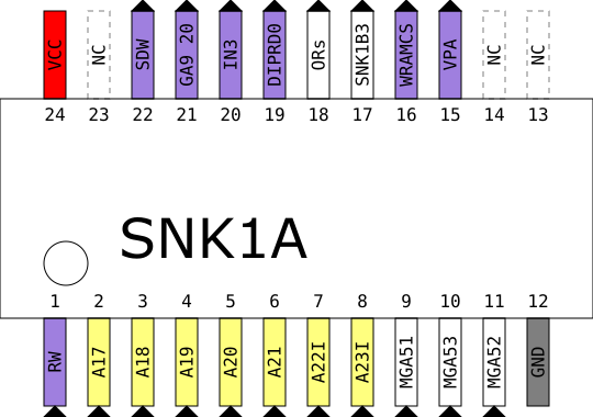
SNK1A
Does some address decoding. Pin 1 might be AS instead of RW.
JEDEC file: File:SNK1A.zip
SNK1B
Generates the DTACK signal.
JEDEC file: File:SNK1B.zip

