Super MVS convertor II: Difference between revisions
Jump to navigation
Jump to search
(Created page with "<div align="center"> <gallery widths=400px perrow=2> File:SMC2_progtop.jpg|Prog board top File:SMC2_progbot.jpg|Prog board bottom File:SMC2_chatop.jpg|CHA board top File:SMC2_...") |
(No difference)
|
Revision as of 20:34, 25 September 2012
-
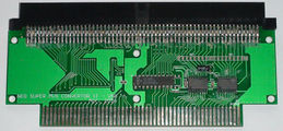
Prog board top
-
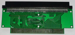
Prog board bottom
-
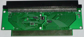
CHA board top
-
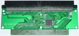
CHA board bottom


Uses a PAL18CV8 and two LS245 transceivers on the prog board. Two corresponding footprints for SIL pull-up resistors on the MVS side are left unpopulated.
Unrouted signals:
- 4MB (MVS B34)
- SLOTCS (MVS A42)
Uses a custom chip marked Neo Cell KS300 8436020333002 06-03 to simulate PRO-CT0 logic. An RC circuit (potentiometer) is used to delay the EVEN signal ?
According to [these pictures], the chip would be a custom marked Altera MAX EPM240 PLD. (Boundary scan device ID replies: BB085040 (EPM240 signature reversed) and the header on the back is for JTAG:
| TMS | TDO | GND |
| TDI | TCK | 3.3V |