Super MVS convertor II
-
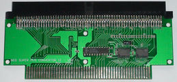
Prog board top
-
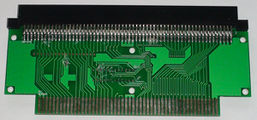
Prog board bottom
-
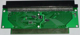
CHA board top
-
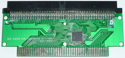
CHA board bottom


Uses a PAL18CV8 and two LS245 transceivers for the 68k data bus on the prog board. Two corresponding footprints for SIL pull-up resistors on the MVS side are left unpopulated.
Unrouted signals:
Uses a chip marked Neo Cell KS300 8436020333002 06-03 to simulate PRO-CT0 logic. An RC circuit (potentiometer) is used to delay the EVEN signal.
The chip is actually a custom marked Altera MAX EPM240 CPLD. Boundary scan device ID replies BB085040 (EPM240 signature reversed) and the header on the back is for JTAG:
| TMS | TDO | GND |
| TDI | TCK | 3.3V |