NEO-DCR-T: Difference between revisions
Jump to navigation
Jump to search
mNo edit summary |
m (→Pinout) |
||
| (3 intermediate revisions by the same user not shown) | |||
| Line 8: | Line 8: | ||
}} | }} | ||
Chip found on late [[MVS hardware|MVS]] boards and next to the [[Hardware DIPs|DIP switches]] on [[ROM-Only boards]]. | |||
* Address decoding | |||
* Coin I/O | |||
* [[Memory_mapped_registers#System_registers|System register]] | |||
* [[Wait cycle]] generator | |||
=Pinout= | =Pinout= | ||
{{Pinout|NEO-DCR|900}} | |||
* DIPRD0 and DIPRD1 go to a {{Chipname|NEO-BUF}} chip to gate the remaining DIP switch bits and RTC inputs | |||
* Pin 85 might be an input | |||
* No [[memory card]] control signals ? | |||
[[Category:Chips]] | [[Category:Chips]] | ||
Latest revision as of 01:58, 8 July 2018

| |
| Package | QFP100R |
| Manufacturer | |
| First use | 1995 ? |
| Used on | MV1B ... |
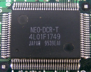
Chip found on late MVS boards and next to the DIP switches on ROM-Only boards.
- Address decoding
- Coin I/O
- System register
- Wait cycle generator
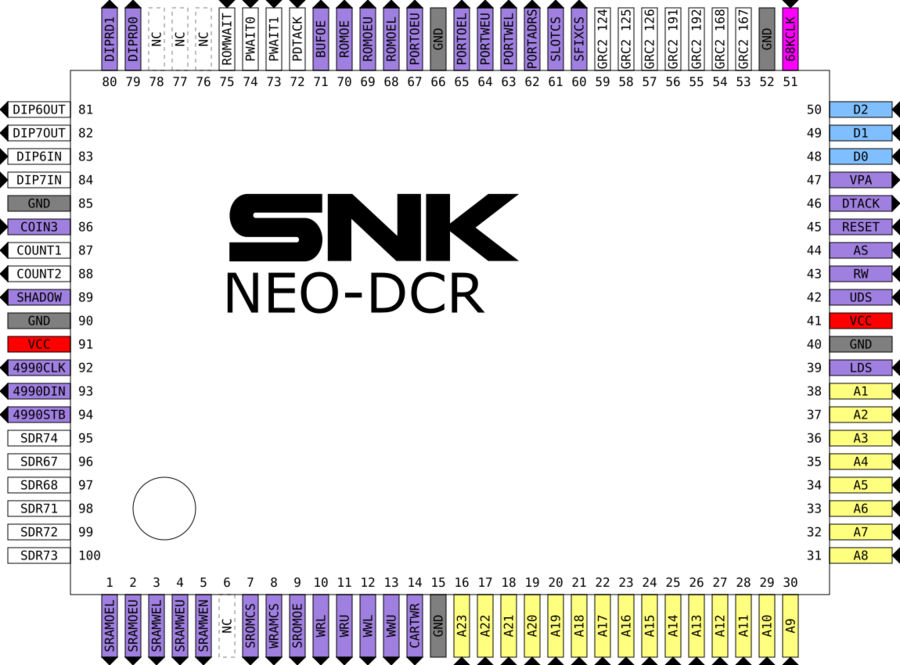
Pinout
- DIPRD0 and DIPRD1 go to a NEO-BUF chip to gate the remaining DIP switch bits and RTC inputs
- Pin 85 might be an input
- No memory card control signals ?
