NEO-257: Difference between revisions
mNo edit summary |
(Repair tips) |
||
| (11 intermediate revisions by the same user not shown) | |||
| Line 1: | Line 1: | ||
{{ChipInfo | |||
|picture=Neo-257.jpg | |||
|pkg=QFP64R | |||
|manu=fujitsu | |||
|date=1990 ? | |||
|gates= | |||
|used_on={{PCB|MV2B}}... | |||
}} | |||
Four "74HC257" quad 2-to-1 multiplexers with a common select line and separate output enables. | |||
Makes 16 switches in one chip (32 inputs, 16 outputs). | |||
== MV2B @ K4 | Used in dual slot MVS systems to switch between carts. | ||
Select signal comes from one of the "SLOT" outputs of {{Chipname|NEO-F0}} ? | |||
=Internal logic= | |||
'''This is NOT verified'''. | |||
See https://github.com/neogeodev/SNKVerilog/tree/master/NEO-257 | |||
=Repair= | |||
The NEO-257 is known to fail on damaged [[MV2B]] and [[MV2F]] boards. If some pins are dead, they can be lifted and wired to a 74LS257. '''These instructions only work for the MV2B chips at L4 and K4'''. | |||
* Wire the NEO-257 data inputs to any of the 74LS257 input pairs (in correct order). | |||
* Wire the 74LS257 output to the output pad. | |||
* Wire the NEO-257 pin 17 to the 74LS257 select input. | |||
* Wire power, the 74LS257 output enable to ground, and don't forget to ground the unused inputs if using a CMOS part. | |||
=Pinouts= | |||
Information provided by Channelmaniac. '''Pins 2 and 3 could be "enable" pins'''. | |||
* A*, B*: Inputs | |||
* Y*: Outputs | |||
* 17 SELECT: A if low, B if high | |||
* 18 is an active low output enable for Y0~Y7 | |||
* 33 and 34 are probably ORed together to provide an active low output enable for Y8~Y15 | |||
* 35 is an active high enable for entire chip | |||
==MV2B @ L4== | |||
Used to switch the upper 16 bits of the sprite graphics bus. | |||
[[File:Neo-257_L4_pinout.png|512px]] | |||
OpenOffice Draw file: [[File:neo-257_L4.odg]] | |||
== MV2B @ K4== | |||
Used to switch the lower 16 bits of the sprite graphics bus. | |||
[[File:Neo-257_K4_pinout.png|512px]] | [[File:Neo-257_K4_pinout.png|512px]] | ||
| Line 12: | Line 58: | ||
OpenOffice Draw file: [[File:neo-257_K4.odg]] | OpenOffice Draw file: [[File:neo-257_K4.odg]] | ||
== MV2B @ J11 | == MV2B @ J11== | ||
SYSTEM and SYSTEMB might be reversed ? | |||
[[File:Neo-257_J11_pinout.png|512px]] | [[File:Neo-257_J11_pinout.png|512px]] | ||
| Line 18: | Line 66: | ||
OpenOffice Draw file: [[File:neo-257_J11.odg]] | OpenOffice Draw file: [[File:neo-257_J11.odg]] | ||
[[Category:Chips]] | [[Category:Chips]] | ||
[[Category:Repairs]] | |||
Latest revision as of 02:40, 28 November 2018

| |
| Package | QFP64R |
| Manufacturer | |
| First use | 1990 ? |
| Used on | MV2B... |
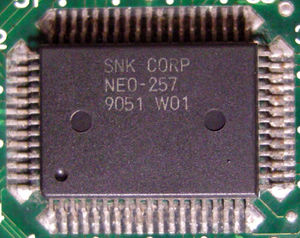
Four "74HC257" quad 2-to-1 multiplexers with a common select line and separate output enables.
Makes 16 switches in one chip (32 inputs, 16 outputs).
Used in dual slot MVS systems to switch between carts.
Select signal comes from one of the "SLOT" outputs of NEO-F0 ?
Internal logic
This is NOT verified.
See https://github.com/neogeodev/SNKVerilog/tree/master/NEO-257
Repair
The NEO-257 is known to fail on damaged MV2B and MV2F boards. If some pins are dead, they can be lifted and wired to a 74LS257. These instructions only work for the MV2B chips at L4 and K4.
- Wire the NEO-257 data inputs to any of the 74LS257 input pairs (in correct order).
- Wire the 74LS257 output to the output pad.
- Wire the NEO-257 pin 17 to the 74LS257 select input.
- Wire power, the 74LS257 output enable to ground, and don't forget to ground the unused inputs if using a CMOS part.
Pinouts
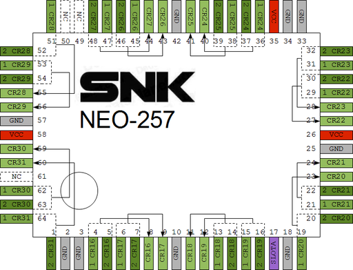
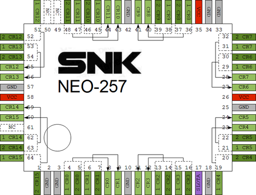
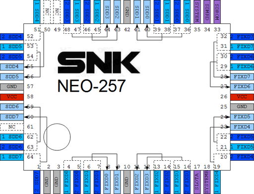
Information provided by Channelmaniac. Pins 2 and 3 could be "enable" pins.
- A*, B*: Inputs
- Y*: Outputs
- 17 SELECT: A if low, B if high
- 18 is an active low output enable for Y0~Y7
- 33 and 34 are probably ORed together to provide an active low output enable for Y8~Y15
- 35 is an active high enable for entire chip
MV2B @ L4
Used to switch the upper 16 bits of the sprite graphics bus.
OpenOffice Draw file: File:Neo-257 L4.odg
MV2B @ K4
Used to switch the lower 16 bits of the sprite graphics bus.
OpenOffice Draw file: File:Neo-257 K4.odg
MV2B @ J11
SYSTEM and SYSTEMB might be reversed ?
OpenOffice Draw file: File:Neo-257 J11.odg


