NEO-F0: Difference between revisions
Jump to navigation
Jump to search
m (ChipInfo) |
No edit summary |
||
| (One intermediate revision by one other user not shown) | |||
| Line 5: | Line 5: | ||
|date=1991 ? | |date=1991 ? | ||
|gates= | |gates= | ||
|used_on={{PCB|MV1FZS}} ... | |used_on={{PCB|MV1FZS}} {{PCB|MV1-1}} ... | ||
}} | }} | ||
| Line 19: | Line 19: | ||
=Pinout= | =Pinout= | ||
{{Pinout|NEO-F0|640px}} | |||
=Signals= | =Signals= | ||
Latest revision as of 10:50, 18 November 2018

| |
| Package | QFP64R |
| Manufacturer | |
| First use | 1991 ? |
| Used on | MV1FZS MV1-1 ... |
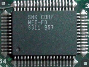
MVS specific chip.
- RTC interface
- Hardware DIPs and cab switches reading
- Coin counters interface
- LEDs and marquee outputs
- Slot selection for multi-slot boards
Note: SYSTEMB is used to gate the SLOT* outputs.
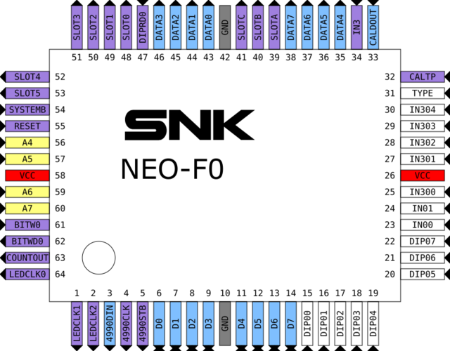
Pinout
Signals
CPU
- A4~A7: 68k address bus
- D0~D7: 68k data bus
RTC
4990*: uPD4990 RTC interface
IN3 DIPRD1: Output IN300~IN304 to D0~D4 and CALTP/CALDOUT to D6/D7 (read $320001). D5 is IN00 ?
I/O
DIPRD0: Output to D0~D7 depending on state of A7:
- A7 low: output dipswitch states DIP00~DIP07 (read $300001)
- A7 high: output IN01 to D7 (test switch) and TYPE to D6 (read $300081)
Slot select
- SLOTA~SLOTC: binary slot selection
- SLOT0~SLOT5: decoded slot selection (active low)
Connections
MV1F:
- IN00: Ground
- IN01: Test switch
- IN300: P1 Coin switch
- IN301: P2 Coin switch
- IN302: Service switch
- IN303/IN304: VCC
MV2B:
- IN303: NEO-E0 H6 50 (BNK0)
- IN304: 3 of PRO-C0, NEO-E0 H6 48
