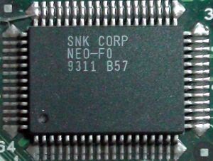
NEO-F0: Difference between revisions
Jump to navigation
Jump to search
mNo edit summary |
mNo edit summary |
||
| Line 16: | Line 16: | ||
*SLOT*: /CS for multislot boards ? | *SLOT*: /CS for multislot boards ? | ||
*DIP00~DIP07: [[DIPs|Dipswitch]] inputs | *DIP00~DIP07: [[DIPs|Dipswitch]] inputs | ||
*IN3: Output IN300~IN302 | *IN3: Output IN300~IN302 to D0~D2 and CALDIF/CALDOUT to D6/D7 (read $320001) | ||
*DIPRD: Output to D0~D7 depending on state of A7 (from | *DIPRD: Output to D0~D7 depending on state of A7 (from | ||
** A7 is low: output DIP00~DIP07 (read $300001) | ** A7 is low: output DIP00~DIP07 (read $300001) | ||
Revision as of 07:02, 13 April 2012

MVS specific chip.
Handles the UPD4990 calendar access, dipswitches, cab switches (test, service...), coin counters, LED marquee outputs and slot selection signals for multi-slot boards.
Pinout
OpenOffice Draw file: File:Neo-f0.odg
- A4~A7: 68k address bus
- D0~D7: 68k data bus
- 4990: uPD4990 RTC interface
- DATA0~DATA7: LED marquee latch data
- SLOT*: /CS for multislot boards ?
- DIP00~DIP07: Dipswitch inputs
- IN3: Output IN300~IN302 to D0~D2 and CALDIF/CALDOUT to D6/D7 (read $320001)
- DIPRD: Output to D0~D7 depending on state of A7 (from
- A7 is low: output DIP00~DIP07 (read $300001)
- A7 is high: output IN01 on D7 (test switch) and TYPE? on D6 (read $300081)
- BITW0: writes to $3800x1 region...(fill in)
- SLOTA~SLOTC: slot selection?
- SLOT0~SLOT5: decoded slot selection? (SLOT0 mislabelled as SLOTD in pic)
MV1F:
- IN00: Ground
- IN01: Test switch
- IN300: P1 Coin switch
- IN301: P2 Coin switch
- IN302: Service switch
- IN303/IN304: VCC