NEO-G0: Difference between revisions
Jump to navigation
Jump to search
m (select info from my 2F) |
m (corrected pins) |
||
| Line 17: | Line 17: | ||
*PAUD0~PAUD7: upper byte of palette data | *PAUD0~PAUD7: upper byte of palette data | ||
*MCD0~MCD15: memory card data bus | *MCD0~MCD15: memory card data bus | ||
*(51) is | *(51) is "enable MCD0~MCD15" pin | ||
*(39) is "enable PALD0~PALD15" pin (confirmed on MV-2F chip used as ADPCM-A multiplexer): | |||
**NEO-F0 -> NEO-G0 @ K9: | |||
**SLOT0(48) -> SEL?(51) | |||
**SLOT1(49) -> "PAL"(39) | |||
[[Category:Chips]] | [[Category:Chips]] | ||
Revision as of 09:29, 9 May 2012

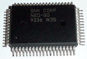
Gates the 68k data bus to the memory card slot and palette RAM. Only found in AES systems ?
PROG B22 (AES cart ROMOE ?) = ROMOEU AND ROMOEL like in NEO-E0 ?
PALWE = PAL OR R/W.
Pinout
OpenOffice Draw file: File:Neo-g0.odg
- D0~D15: 68k data bus
- PALD0~PALD7: lower byte of palette data
- PAUD0~PAUD7: upper byte of palette data
- MCD0~MCD15: memory card data bus
- (51) is "enable MCD0~MCD15" pin
- (39) is "enable PALD0~PALD15" pin (confirmed on MV-2F chip used as ADPCM-A multiplexer):
- NEO-F0 -> NEO-G0 @ K9:
- SLOT0(48) -> SEL?(51)
- SLOT1(49) -> "PAL"(39)