NEO-257: Difference between revisions
Jump to navigation
Jump to search
mNo edit summary |
mNo edit summary |
||
| Line 5: | Line 5: | ||
Select signal comes from one of the "SLOT" outputs of [[NEO-F0]] ? | Select signal comes from one of the "SLOT" outputs of [[NEO-F0]] ? | ||
== MV2B @ K4 pinout== | |||
[[File:Neo-257_K4_pinout.png|512px]] | |||
OpenOffice Draw file: [[File:neo-257_K4.odg]] | |||
== MV2B @ J11 pinout== | |||
[[File:Neo-257_J11_pinout.png|512px]] | |||
OpenOffice Draw file: [[File:neo-257_J11.odg]] | |||
== Pinout == | == Pinout == | ||
Information provided by Channelmaniac. | Information provided by Channelmaniac. | ||
[[File:Neo-257_pinout.png]] | [[File:Neo-257_pinout.png|512px]] | ||
OpenOffice Draw file: [[File:neo-257.odg]] | OpenOffice Draw file: [[File:neo-257.odg]] | ||
Revision as of 22:59, 13 August 2012

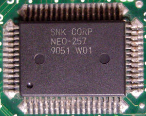
Quadruple 74HC257 2-to-1 multiplexer with common select line, making 16 switches in one chip. Used in dual slot MVS systems to select one of the two C ROM (and S ROM ?) buses.
Select signal comes from one of the "SLOT" outputs of NEO-F0 ?
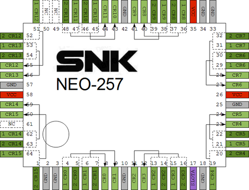
MV2B @ K4 pinout
OpenOffice Draw file: File:Neo-257 K4.odg
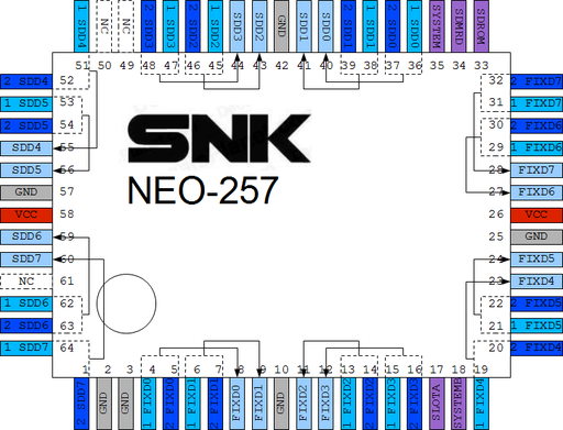
MV2B @ J11 pinout
OpenOffice Draw file: File:Neo-257 J11.odg
Pinout
Information provided by Channelmaniac.
OpenOffice Draw file: File:Neo-257.odg
- A*,B*: Inputs
- Y*: Outputs
- Select: Output A if LOW, B if HIGH.
- Some pins marked as ground could be "enable" pins
- 35 is active high enable for entire chip
- 18 is active low enable for Y0~Y7 (comes from "SYSTEMB" on a MV-2F and used to control /OE for FIXD0~FIXD7 from cart)
- 33 is active low enable for Y8~Y15 (comes from "SDROM" from NEO-D0 to output cart M1 data to Z80)

