NEO-D0: Difference between revisions
Jump to navigation
Jump to search
m (ChipInfo) |
No edit summary |
||
| Line 8: | Line 8: | ||
}} | }} | ||
*Clock divider | * Clock divider | ||
*{{Chipname|Z80}} memory and [[Z80 port map|port]] control | * {{Chipname|Z80}} memory and [[Z80 port map|port]] control | ||
*{{Chipname|YM2610}} interface | * {{Chipname|YM2610}} interface | ||
*[[Memory card]] bank selection | * [[Memory card]] bank selection | ||
*[[Joypad]] outputs | * [[Joypad]] outputs | ||
Maybe similar to {{Chipname|NEO-SUD}} on the NeoGeo CD. Close to the audio hardware. | Maybe similar to {{Chipname|NEO-SUD}} on the NeoGeo CD. Close to the audio hardware. | ||
| Line 20: | Line 20: | ||
OpenOffice Draw file: [[File:neo-d0.odg]] | OpenOffice Draw file: [[File:neo-d0.odg]] | ||
=Internal schematic= | |||
[[File:Neo-d0_sd.png]] | |||
=Signals= | =Signals= | ||
* | * {{Sig|D*|D*}}: {{Chipname|68k}} data bus for [[joypad]] outputs | ||
* | * {{Sig|BNK*|BNK*}}: [[Memory card]] upper address lines to {{Chipname|NEO-E0}} | ||
*A4: 68k address line | * {{Sig|A4|A4}}: 68k address line for decoding | ||
*4116CS: Z80 RAM | * {{Sig|4116CS|4116CS}}: [[Z80 RAM]] select | ||
*2610*: YM2610 control | * 2610*: YM2610 control outputs | ||
* | * {{Sig|OUT*|OUT*}}: Joypad outputs | ||
*SDMRD/SDMRW: Z80 | * {{Sig|SDMRD|SDMRD}}: Z80 ROM/RAM read | ||
* | * {{Sig|SDMRW|SDMRW}}: Z80 RAM write | ||
* | * {{Sig|SDRD*|SDRD*}}: Z80 port read to {{Chipname|NEO-ZMC}} in cartridge | ||
* {{Sig|SDZ80CLR|SDZ80CLR}}: Clear command code in {{Chipname|NEO-C1}} | |||
* {{Sig|SDZ80RD|SDZ80RD}}: Read command code from {{Chipname|NEO-C1}} | |||
* {{Sig|SDZ80WR|SDZ80WR}}: Write reply code to {{Chipname|NEO-C1}} | |||
[[Category:Chips]] | [[Category:Chips]] | ||
Revision as of 07:51, 19 February 2017

| |
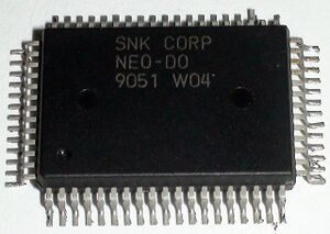
| Package | QFP64R |
| Manufacturer | |
| First use | 1990 ? |
| Used on | MV4 and many more... |
- Clock divider
- Z80 memory and port control
- YM2610 interface
- Memory card bank selection
- Joypad outputs
Maybe similar to NEO-SUD on the NeoGeo CD. Close to the audio hardware.
Pinout
OpenOffice Draw file: File:Neo-d0.odg
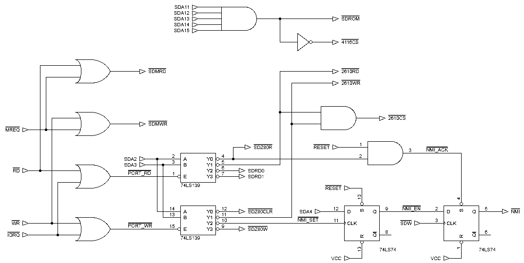
Internal schematic
Signals
- D*: 68k data bus for joypad outputs
- BNK*: Memory card upper address lines to NEO-E0
- A4: 68k address line for decoding
- 4116CS: Z80 RAM select
- 2610*: YM2610 control outputs
- OUT*: Joypad outputs
- SDMRD: Z80 ROM/RAM read
- SDMRW: Z80 RAM write
- SDRD*: Z80 port read to NEO-ZMC in cartridge
- SDZ80CLR: Clear command code in NEO-C1
- SDZ80RD: Read command code from NEO-C1
- SDZ80WR: Write reply code to NEO-C1
