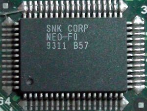
NEO-F0: Difference between revisions
Jump to navigation
Jump to search
No edit summary |
mNo edit summary |
||
| Line 5: | Line 5: | ||
Handles the [[UPD4990]] calendar access, dipswitches, cab switches (test, service...), coin counters, LED marquee outputs and slot selection signals for multi-slot boards. | Handles the [[UPD4990]] calendar access, dipswitches, cab switches (test, service...), coin counters, LED marquee outputs and slot selection signals for multi-slot boards. | ||
=Pinout= | |||
[[File:neo-f0_pinout.png]] | |||
*A4~A7: [[68k]] address bus | |||
*D0~D7: 68k data bus | |||
*4990: [[uPD4990]] RTC interface | |||
*DATA0~DATA7: LED marquee latch data | |||
*SLOT*: /CS for multislot boards ? | |||
*DIP00~DIP07: [[DIPs|Dipswitch]] inputs | |||
MV1F: | |||
*IN00: Ground | |||
*IN01: Test switch | |||
*IN300: P1 Coin switch | |||
*IN301: P2 Coin switch | |||
*IN302: Service switch | |||
*IN303/IN304: VCC | |||
[[Category:Chips]] | [[Category:Chips]] | ||
Revision as of 08:45, 14 March 2011

MVS specific chip.
Handles the UPD4990 calendar access, dipswitches, cab switches (test, service...), coin counters, LED marquee outputs and slot selection signals for multi-slot boards.
Pinout
- A4~A7: 68k address bus
- D0~D7: 68k data bus
- 4990: uPD4990 RTC interface
- DATA0~DATA7: LED marquee latch data
- SLOT*: /CS for multislot boards ?
- DIP00~DIP07: Dipswitch inputs
MV1F:
- IN00: Ground
- IN01: Test switch
- IN300: P1 Coin switch
- IN301: P2 Coin switch
- IN302: Service switch
- IN303/IN304: VCC