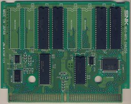
CHA256: Difference between revisions
Jump to navigation
Jump to search
mNo edit summary |
No edit summary |
||
| Line 12: | Line 12: | ||
!Jumper set | !Jumper set | ||
|- | |- | ||
| | |1MiB | ||
|J5+J6 | |J5+J6 | ||
|- | |- | ||
| | |2MiB | ||
|J7+J8 | |J7+J8 | ||
|- | |- | ||
| | |4MiB | ||
|J9+J10 | |J9+J10 | ||
|} | |} | ||
A [[NEO-273]] and a LS74 are used to address C ROM. The LS74 provides the 2 most significant bits. The LS139 enables one of four pairs of C ROMs using 2 address inputs depending on which 2 jumpers are connected. | A [[NEO-273]] and a LS74 are used to address C ROM. The LS74 provides the 2 most significant bits. The LS139 enables one of four pairs of C ROMs using 2 address inputs depending on which 2 jumpers are connected. | ||
*Max 256Mbit C ROM (8x 32Mbit) | |||
*[[NEO-273]] | |||
*[[NEO-ZMC]] | |||
*LS139,LS74 | |||
==AES version== | |||
{| class="wikitable" | {| class="wikitable" | ||
|- | |- | ||
! | !C ROM type | ||
! | !Jumper set | ||
|- | |||
|<4MiB | |||
|J15+J16+J17+J18 | |||
|- | |- | ||
| | |4MiB | ||
| | |J11+J12+J13+J14 | ||
|} | |} | ||
{| class="wikitable" | {| class="wikitable" | ||
|- | |- | ||
! | !M1 ROM size | ||
! | !Jumper set | ||
|- | |||
|64KiB | |||
|J1+J4 | |||
|- | |- | ||
| | |128KiB | ||
| | |J2+J3 | ||
|} | |} | ||
{| class="wikitable" | |||
|- | |||
!EVEN delay | |||
!Jumper set | |||
|- | |||
|1 gate | |||
|J19 | |||
|- | |||
|2 gates | |||
|J20 | |||
|} | |||
[[Category:Cartridge boards]] | [[Category:Cartridge boards]] | ||
Revision as of 18:27, 15 January 2013

C ROMs
Up to 8 * 32Mbit ROMs (27C322) can be used for a maximum of 256Mbit. 27C800/27C160 can also be used depending on jumper configuration.
The size of largest ROM is selected using a pair of jumpers. The rest should be left unconnected.
| Largest C ROM | Jumper set |
|---|---|
| 1MiB | J5+J6 |
| 2MiB | J7+J8 |
| 4MiB | J9+J10 |
A NEO-273 and a LS74 are used to address C ROM. The LS74 provides the 2 most significant bits. The LS139 enables one of four pairs of C ROMs using 2 address inputs depending on which 2 jumpers are connected.
AES version
| C ROM type | Jumper set |
|---|---|
| <4MiB | J15+J16+J17+J18 |
| 4MiB | J11+J12+J13+J14 |
| M1 ROM size | Jumper set |
|---|---|
| 64KiB | J1+J4 |
| 128KiB | J2+J3 |
| EVEN delay | Jumper set |
|---|---|
| 1 gate | J19 |
| 2 gates | J20 |