PROGBK1: Difference between revisions
mNo edit summary |
m (27c322 has no 8bit mode) |
||
| Line 90: | Line 90: | ||
[[File:Progbk1v.png]] | [[File:Progbk1v.png]] | ||
There is a maximum of 4 [[V ROM]]s which can be 8Mbit, 16Mbit or 32Mbit (27C800/27C160 | There is a maximum of 4 [[V ROM]]s which can be 8Mbit, 16Mbit or 32Mbit (27C800/27C160) for a maximum total size of 4 * 4MiB = 16MiB. | ||
A 4Mbit ROM can also be used, but only if there's one and only if it's in the last used slot. | A 4Mbit ROM can also be used, but only if there's one and only if it's in the last used slot. | ||
Revision as of 18:38, 31 July 2014
The only non-protected board that can bankswitch and use all V ROM space. Really common and very useful for homebrew stuff or converts.
P ROMs
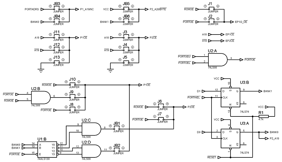
| J1 | J2 |
|---|---|
| EP ROMs /OE are /ROMOE | EP ROMs /OE are /PORTOE |
| J3 | J4 | J5 |
|---|---|---|
| P2 /CE is A18 | P2 /CE is /A18 | P2 /CE is GND (default) |
| J6 | J7 | JB1 |
|---|---|---|
| P2 /OE is /ROMOE | P2 /OE is /PORTOE (default) | P2 /OE is /PORTOE, banks 0 and 1 |
| J8 | J9 | J10 | JB2 |
|---|---|---|---|
| P1 /OE is /PORTOE | P1 /OE is /PORTOE AND /ROMOE | P1 /OE is /ROMOE (default) | P1 /OE is /PORTOE, banks 2 and 3 |
| J11 | J12 | J13 |
|---|---|---|
| P1 /CE is A18 | P1 /CE is /A18 | P1 /CE is GND (default) |
| JB3 | JB4 | Nothing |
|---|---|---|
| P1 A19/NC is /PORTADRS | P1 A19/NC is BANK0 (P1 is 16Mbit) | P1 is 8Mbit |
| JB5 | JB6 |
|---|---|
| P2 A20//BYTE is VCC (P2 is 16Mbit or less) | P2 A20//BYTE is BANK1 (P2 is 32Mbit) |
The P1 ROM can be 4Mbit, 8Mbit or 16Mbit (27C400/27C800/27C160).
- ROMs can be halved and mapped to 0x000000~0x0FFFFF or 0x200000~0x2FFFFF.
- If P1 is 4Mbit or 8Mbit, then P2 can contain a bankswitched ROM (same type as P1 plus 27C322). P1 appears in 0x000000~0x0FFFFF. P2 bank appears in 0x200000~0x2FFFFF.
Bankswitching is done with the LS74. It's not needed if the game isn't banked. Any write to an odd address in the 0x200000~0x2FFFFF range will set the bank.
V ROM
There is a maximum of 4 V ROMs which can be 8Mbit, 16Mbit or 32Mbit (27C800/27C160) for a maximum total size of 4 * 4MiB = 16MiB.
A 4Mbit ROM can also be used, but only if there's one and only if it's in the last used slot.
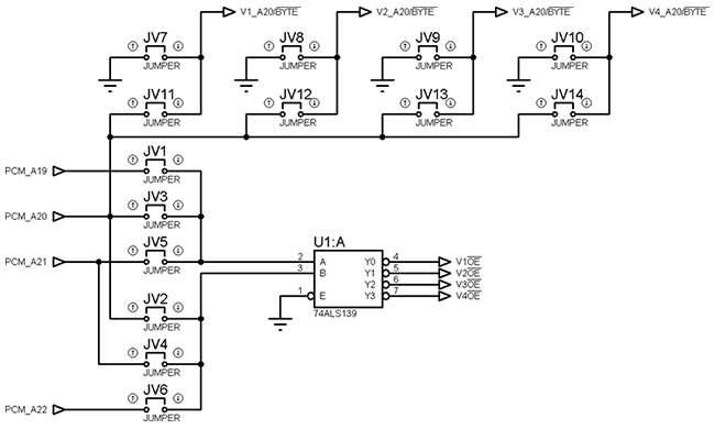
The size of the largest V ROM is selected with a pair of jumpers on 6 spots (3 possible choices).
| Largest V ROM | Jumper set |
|---|---|
| 8Mbit (1MiB) | JV1+JV2 |
| 16Mbit (2MiB) | JV3+JV4 |
| 32Mbit (4MiB) | JV5+JV6 |
This pair of V ROM jumpers effectively choose a set of 2 of the PCM chip address outputs to input to the LS139, which will enable one out of the 4 V ROMs at a time.
The JV7 to JV14 jumpers need to be set according to the ROM types. If it's less than 32Mbit, the JV7/JV8/JV9/JV10 jumper needs to be set (ground). If it's 32Mbit, the JV11/JV12/JV13/JV14 needs to be set (A20). This is because 32Mbit chips have their /BYTE pin replaced by A20.
Other
The LS08 is used to AND the /PORTOEU and /PORTOEL signals to get a /PORTOE.
- 4x 1/2/4MiB V ROMs
- 1/2MiB P1 ROM
- 1/2/4MiB P2 ROM
- 2x 512KiB EP1/EP2 ROM
- PCM chip
- LS139,LS08,LS74

