LSPC-A0: Difference between revisions
Jump to navigation
Jump to search
mNo edit summary |
mNo edit summary |
||
| Line 1: | Line 1: | ||
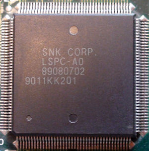
[[File:Mvs_lspc-a0.jpg|right|thumb|LSPC-A0 graphics chip found | [[File:Mvs_lspc-a0.jpg|right|thumb|LSPC-A0 graphics chip found on a [[MV4]] board.]] | ||
LSPC-A0 is the [[VDC]] part of the first generation chipset, see {{Chipname|LSPC2-A2}} for more details. | |||
=Pinout= | =Pinout= | ||
117: 8 ULN2803 K11 / 112 C0 | *117: 8 ULN2803 K11 / 112 C0 | ||
116: C0 109 | *116: C0 109 | ||
115: C0 110 | *115: C0 110 | ||
124: 2H1 | *124: 2H1 | ||
125: CA4 | *125: CA4 | ||
126: F7 LS86 12 | *126: F7 LS86 12 | ||
127: C0 37/1 Ls273 E4/5 | *127: C0 37/1 Ls273 E4/5 | ||
128: C0 54/B0 21 | *128: C0 54/B0 21 | ||
158: 3 D7 (AS04) | *158: 3 D7 (AS04) | ||
[[File:lspc-a0_pinout.png|640px]] | [[File:lspc-a0_pinout.png|640px]] | ||
| Line 22: | Line 21: | ||
*A1~A3: {{Chipname|68k}} address bus | *A1~A3: {{Chipname|68k}} address bus | ||
*D0~D15: 68k data bus | *D0~D15: 68k data bus | ||
*SVA0~SVA14: Slow VRAM bank address bus | *SVA0~SVA14: Slow [[VRAM]] bank address bus | ||
*SVD0~SVD15: Slow VRAM bank data bus | *SVD0~SVD15: Slow VRAM bank data bus | ||
*FVA0~FVA10: Fast VRAM bank address bus | *FVA0~FVA10: Fast VRAM bank address bus | ||
*FVD0~FVD15: Fast VRAM bank data bus | *FVD0~FVD15: Fast VRAM bank data bus | ||
[[Category:Chips]] | [[Category:Chips]] | ||
Revision as of 10:40, 19 August 2016

LSPC-A0 is the VDC part of the first generation chipset, see LSPC2-A2 for more details.
Pinout
- 117: 8 ULN2803 K11 / 112 C0
- 116: C0 109
- 115: C0 110
- 124: 2H1
- 125: CA4
- 126: F7 LS86 12
- 127: C0 37/1 Ls273 E4/5
- 128: C0 54/B0 21
- 158: 3 D7 (AS04)
OpenOffice Draw file: File:Lspc-a0.odg