NEO-D0: Difference between revisions
Jump to navigation
Jump to search
mNo edit summary |
m (ChipInfo) |
||
| Line 1: | Line 1: | ||
{{ChipInfo | |||
|picture=aes_d0.jpg | |||
|pkg=QFP64R | |||
|manu=fujitsu | |||
|date=1990 ? | |||
|gates= | |||
|used_on={{PCB|MV4}} and many more... | |||
}} | |||
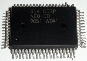
*Clock divider | *Clock divider | ||
Revision as of 01:11, 12 October 2016

| |
| Package | QFP64R |
| Manufacturer | |
| First use | 1990 ? |
| Used on | MV4 and many more... |
- Clock divider
- Z80 memory and port control
- YM2610 interface
- Memory card bank selection
- Joypad outputs
Maybe similar to NEO-SUD on the NeoGeo CD. Close to the audio hardware.
Pinout
OpenOffice Draw file: File:Neo-d0.odg
Signals
- D0~D5: 68k data bus for joypad outputs
- BNK0~BNK2: Memory card upper address lines to NEO-E0
- A4: 68k address line
- 4116CS: Z80 RAM /CS
- 2610*: YM2610 control lines
- OUT1~OUT6: Joypad outputs
- SDMRD/SDMRW: Z80 ROM/RAM control lines
- SDRD0/SDRD1: Z80 port reads to NEO-ZMC in cartridge
- SDZ80*: Control lines to NEO-C1